of the SLIM MSA
Page Started 11-01-09.
Updated 10-1-15.
You came to this page because:
A. You are interested in the technical aspects of the MSA.
B. Your MSA is not functioning properly and need some troubleshooting guidance.
C. You are learning about RF circuits and crave for more information.
D. You are an RF guru and want to critique my design. OK, that's fine, I'm not perfect and I make mistakes. E-mail me and offer suggested improvements.
E. You pushed the wrong button. You think "RF" means Redwood Fence. Use your browser's "Back" button and leave before your brain turns to mush.
This Technical Analysis of the MSA is for those who are interested in the inner workings of the MSA. It can be helpful for troubleshooting the MSA. This page will be divided into sections:
System Description
Block Diagram
The Basic MSA, the Spectrum Analyzer
The MSA with Tracking Generator
The Vector Network Analyzer
System Analysis
MSA Gain
Input Sensitivity
Maximum Input Power Level
Input Dynamic Range
MSA Input Noise Floor
Other Factors Affecting Analysis
Module Analysis
Local Oscillator Output Levels and Mixer Drive
Control Board using SLIM-CB-NV
Mixer 1, the Input Stage of the MSA
Mixer 1, Isolation
MSA Phase Noise Contribution to Signal Magnitude Measurements
MSA Phase Noise Contribution to Signal Phase Noise Measurements
PLO Phase Noise, General
PLO 1 using SLIM-PLO-1
PLO 3 using SLIM-PLO-1
PLO 2 using SLIM-PLO-2
DDS 1, using SLIM-DDS-107
DDS 3, using SLIM-DDS-107
Mixer 2 using SLIM-MXR-2
I.F. Amplifier using SLIM-IFA-33
Resolution Bandwidth Filter, aka. Final Xtal Filter
Coaxial Cavity Filter
Log Detector using SLIM-LD-8306
A to D Converter, using either a 12 or 16 Bit Serial A to D Converter:
16 Bit Serial A to D Converter using SLIM-ADC-16
12 Bit Serial A to D Converter using SLIM-ADC-12
Mixer 3 using SLIM-MXR-3
Mixer 4 using SLIM-MXR-4
PDM, Phase Detector Module, using SLIM-PDM
Master Oscillator using SLIM-MO-64
Other Stuff
Fan Addition
Spurious, Interference, and other Weird Stuff in the MSA
Spurious Defined
Spur Creation in the Basic Spectrum Analyzer
Spur Creation in the Spectrum Analyzer plus Tracking Generator
Spur Creation in the VNA
Known Spurious Signals and Interference
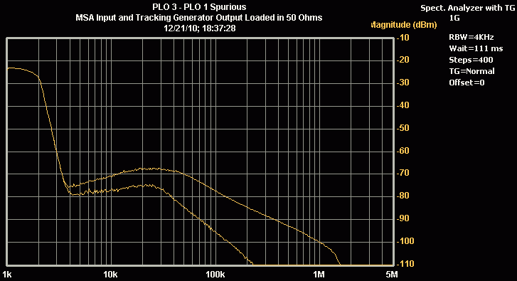
PLO 3 - PLO 1 Spurious
PLO 3 - PLO 2 Spurious
PLO 3 Harmonic Interference
System Description
Block Diagram
There are three MSA configurations. The Basic MSA, the MSA with Tracking Generator addition, and the MSA with VNA extension. This is the block diagram of the MSA with VNA extension.

You will notice that several items within the block diagram do not have committed connections. This is because the MSA can have several bands of operation, and the interconnections depend upon the band of operation. They will be explained in the following paragraphs.
The Basic MSA, the Spectrum Analyzer
Common Configuration for all Bands: A dual conversion topology is used to minimize internally generated spurious. A 10.7 MHz Final I.F. is chosen to take advantage of commercially available filters. The magnitude detector is a logrithmic detector with 100 dB of dynamic range, driving a 16 bit Analog to Digital Converter. There are two local oscillators, LO 1 driving Mixer 1, and LO 2 driving Mixer 2. LO 1 is comprised of a Phase Locked Oscillator (PLO 1) and a Direct Digital Synthesizer (DDS 1), arranged as a hybrid synthesizer. LO 2 is a Phase Locked Oscillator (PLO 2), commanded to a fixed frequency of 1024 MHz. A 64 MHz Master Oscillator is used as the reference. A Control Board interfaces the MSA to the home computer.
1G Band of Operation: The MSA frequency range is from 0 to 1000 MHz and the input is J2 of Mixer 1. PLO 1 is variable, from 1013.3 MHz to 2013.3 MHz, and will high-side mix with the input frequency. The converted output at J3 of Mixer 1 is 1013.3 MHz, and is passed to the Coaxial Cavity Filter for image rejection. Its output is mixed with PLO 2, a fixed frequency of 1024 MHz. to produce the Final I.F. of 10.7 MHz. The final I.F. is low pass filtered within Mixer 2 and is present at J2. The final IF is passed to J3 of the I.F. Amplifier, amplified, and passed to a user selected, Final Xtal Filter. This filter determines the Resolution Bandwidth of the MSA. The magnitude of the signal is converted to a relative voltage by the Log Detector and processed by the Analog to Digital Converter. The digital signal is passed through the Control Board to the home computer for software processing.
3G Band of Operation: The MSA frequency range is from 2000 to 3000 MHz and the input is J2 of Mixer 1. PLO 1 is variable, from 986.7 MHz to 1986.7 MHz, and will low-side mix with the input frequency. The converted output at J3 of Mixer 1 is 1013.3 MHz, and is passed to the Coaxial Cavity Filter for image rejection. Its output is mixed with PLO 2, a fixed frequency of 1024 MHz. to produce the Final I.F. of 10.7 MHz.
The J2 input port of Mixer 1 has degraded performance for input frequencies above 1000 MHz. Although the 3G Band of the MSA is responsive with this configuration, it is better to reverse the input/outport ports of Mixer 1. The MSA input would become J3 of Mixer 1 and the 1st I.F. would exit J2.
2G Band of Operation: The MSA frequency range is from 1000 to 2000 MHz. With a physical change to the path topology, the MSA is changed to a single conversion topology. PLO 1 is variable, from 1010.7 MHz to 2010.7 MHz, and will high-side mix with the input frequency. The converted output at J3 of Mixer 1 is 10.7 MHz, and is passed to the 2G Low Pass Filter. Its output is passed to J3 of the I.F. Amplifier, amplified, and passed to a user selected, Final Xtal Filter. The Coaxial Cavity Filter and Mixer 2 are not used for 2G Band operation.
Again, the J2 input port of Mixer 1 has degraded performance for input frequencies above 1000 MHz. Although the 2G Band is responsive with this configuration, it is better to reverse the input/outport ports of Mixer 1. The MSA input would become J3 of Mixer 1 and the Final I.F. would exit J2.
This single conversion scheme has no image rejection. That is, Mixer 1 will act as a low-side mixer and will produce the same 10.7 MHz conversion frequency for input frequencies of 1021.4 MHz to 2021.4 MHz. This is because input signals can be either 10.7 MHz above LO 1 or 10.7 MHz below LO 1.
The MSA with Tracking Generator
The Tracking Generator is comprised of PLO 2, PLO 3, and Mixer 3. PLO2 (1024 MHz) and PLO 3 (1024 MHz to 2124 MHz) are combined in Mixer 3 to produce the TG Output. For 1G and 3G Band operation, J2 of PLO 3 is connected to J1 of Mixer 3. The TG output is at J2 of Mixer 3.
Subtractive mixing (PLO3-PLO2) produces the TG output range from 0 MHz to 1000 MHz (1G Band). Additive mixing (PLO3+PLO2) produces the TG output range from 2000 MHz to 3000 MHz (3G Band). Also, there are plenty of harmonic products created by Mixer 3. These are too numerous to list and the power levels are uncertain. These multiple TG output signals can be of good use, or they can be detremental. Some form of external filtering must be added to the TG output to attenuate unwanted frequencies. The formula for the Tracking (or Signal) Generator output frequency is TG = Q*PLO 3 + M*PLO 2, where Q and M can be any positive or negative integer number, including zero.
During 2G Band operation, the same Mixer 3 configuration will produce a TG output from 1000 MHz to 2000 MHz. However, the power level will be quite low since there is no "mixing" within Mixer 3. The TG signal is the mixer isolation leakage of PLO 3. It is better to re-configure and use the J2 output of PLO 3 for the Tracking Generator. It will have a power level of approximately +10 dBm.
The Vector Network Analyzer
The VNA extension is comprised of PLO 1, PLO 3, Mixer 4 and the Phase Detector Module (PDM). Mixer 4 output is the difference frequency of PLO 1 and PLO 3. The difference frequency between PLO 1 and PLO 3 will always be the same as the Final I.F. frequency (10.7 MHz). Mixer 4 output is the "Phase Reference" supplied to the PDM. The power level is approximately -10 dBm. The second input of the PDM is supplied by the Limiter section of the Log Detector Module. This is the limited Final I.F. and is the "Phase Signal" that is measured, relative to the Phase Reference. It is a square wave with a level of approximately 30 mvpp. The output of the PDM (Phase Volts) is a DC voltage that is proportional to the differential phase of its two input signals. The Phase Volts is converted to a digital format by the Analog to Digital Converter and passed through the Control Board to the Computer for processing.
System Analysis
MSA Gain
First, approximate gains and losses in the SLIM MSA. Each mixer has -6.5 dB of loss. The coaxial cavity filter has -7 dB of loss. The dual I.F. Amplifier has +40 dB of gain. The loss of the Final Xtal Filter (Resolution Bandwidth Filter) can vary, but for now, assume it has -4 dB loss and a bandwidth of 2.2 KHz. The total MSA gain (from MSA input to Log Detector Module) = -6.5dB -7dB -6.5dB +40dB -4dB = +16 dB. This is a nominal value. Any deviation of the previously mentioned components would change this gain figure. Probably the biggest contributor to gain difference can be attributed to the coaxial cavity filter. Its insertion loss is dependent on its construction and tuning, and can range anywhere between -3 dB to -8 dB. The mixer loss of -6.5 dB is dependent on its LO drive level. Lower drive level will result in greater mixer loss, but it is not dB for dB. Lowering the drive level by 3 dB may only degrade mixer loss by 1 dB. If Mixer 1 has internal attenuation in its input path, the total MSA gain will be reduced by the amount of the attenuator.
Input Sensitivity, Minimum Signal Input Power Level
For the MSA, I define sensitivity as the minimum input signal power that can be measured and quantified. MSA sensitivity is mostly dependent on the sensitivity of the SLIM Log Detector, but the Resolution Bandwidth Filter will play a significant role in determining sensitivity. Its role will be explained in the paragraph "MSA Input Noise Floor". For the following analysis, assume the RBWF is 2.2 KHz.
For Magnitude, this is the input power level that causes the graphed noise floor to increase. Analog Devices specifies the input noise floor of the AD8306 to be -91 dBv (28.18 microvolts). Due to the 1:4 voltage transformation within the Log Detector Module, the input voltage at the 50 ohm input of the SLIM Log Detector Module is 7.045 microvolts (-90 dBm). Using the MSA Gain figure of 16 dB, the minimum signal level at the input to the MSA would be: -90 dBm - 16 dBm = -106 dBm.
For Phase, this is the input power level that causes the Limited RF output of the SLIM Log Detector to deviate more than 2 degrees. Analog Devices specifies this input to the AD8306 to be -73 dBv. This equates to -72 dBm input to the Log Detector Module. Using the MSA Gain figure of 16 dB, the minimum signal level at the input to the MSA would be: -72 dBm - 16 dBm = -88 dBm.
Maximum Input Power Level
There are three quantities to define here. One is the maximum input signal to the MSA without causing destruction. This level is the maximum input to Mixer 1 (ADE-11X) and is +17 dBm (50 mw).
The other two are the maximum input power levels that can be quantified as a Magnitude measurement or a Phase measurement. These levels are mostly dependent on the saturation level of the SLIM Log Detector.
For Magnitude, Analog Devices specifies the maximum input to the AD8306 I.C. to be +9 dBv (2.818 volts). Due to the 1:4 voltage transformation within the Log Detector Module, the input voltage at the 50 ohm input of the SLIM Log Detector Module is .7045 volts (+10 dBm). Using the MSA Gain figure of 16 dB, the maximum signal level at the input to the MSA would be -6 dBm.
For Phase, Analog Devices specifies the maximum input to the AD8306 to be -3 dBv, to preven phase distortion. This equates to -2 dBm input to the Log Detector Module. Using the MSA Gain figure of 16 dB, the maximum signal level at the input to the MSA would be -18 dBm.
Input Dynamic Range
The MSA Dynamic Range is the difference between minimum measurable input signal and the maximum measurable input signal.
For Spectrum Analyzer Mode, the minimum and maximum magnitude levels at the input to the MSA was analyzed be -106 dBm and -6 dBm. This would indicate that the Spectrum Analyzer Input Dynamic Range is 100 dB.
For VNA Mode, the minimum and maximum magnitude level to maintain a constant phase was analyzed be -88 dBm and -18 dBm. This would indicate that the VNA Input Dynamic Range is 70 dB.
However, the previous analysis uses the specifications of the AD8306 Log Detector. In reality, it will operate outside of its specifications and can be characterized. Characterization takes place during MSA Calibration.
MSA Input Noise Floor
The previous analysis for Power Levels and MSA Dynamic Range assumed that the noise floor of the MSA was determined by the Log Detector. This paragraph explains how the analysis is justified.
The Input Noise Floor of the MSA is determined by the self generated noise of all the circuits within the MSA. That is, it is assumed that there is no "real" signal entering the MSA to be measured by the Log Detector. This is a reality if the MSA is commanded to any frequency that does not create spurious signals. Spurs are explained near the end of this page. The devices, Mixer 1 and Mixer 2 do create noise, but their total level is below the physical noise floor of -174 dBm/sqrtHz (a 1 Hz bandwidth).
Therefore, the total noise created in the MSA is the combination of the two I.F. Amplifiers and the Log Detector. The first I.F. Amplifier has a noise figure of 3 dB and a gain of 20 dB. The broad-band noise generated by the first amplifier is = -174dBm +3dB(amp noise figure) +20dB(gain) = -151 dBm /sqrtHz. The second amplifier (20 dB gain) increases the noise to -131 dBm /sqrtHz. This output noise must pass through the Resolution Filter before it enters the Log Detector. The Filter will limit the bandwidth of the noise to the bandwidth of the Filter. The Filter will also reduce the noise by an amount equal to the insertion loss of the Filter. (Assume the bandwidth is 2.2 KHz, with -4 dB loss). The total noise at the input to the Log Det SLIM = -131 dBm /sqrtHz + 10logBW(2.2KHz) - 4dB(filter loss) = -131 +33.4 -4 = -101.6 dBm. This total noise value of -101.6 dBm is much lower than the input noise floor (-90 dBm) of the Log Detector. This means that the Log Detector is determining the noise floor and the previous assumption that the MSA Dynamic Range of 100 dB is valid.
If the 2.2 KHz Final Xtal Filter is replaced with a 15 KHz bandwidth filter, the total noise input to the Log Detector will increase. The total noise at the input to the Log Det will be: Total noise = -174dBm +3dB(amp noise figure) +20dB +20dB +10logBW(15KHz) -4dB(filt loss) = -174+3+40+41.8-4 = -93.2 dBm. This total noise level is 3.2 dB lower than the -90 dBm noise floor of the Log Detector. The Log Detector is still determining the noise floor and the MSA Dynamic Range of 100 dB is still valid.
The question becomes, what is the maximum bandwidth we can use for the Resolution Filter and not add noise.The maximum value of noise bandwidth that can be added between the amplifier output and the Log Detector input is (131-90) = 41 dB. Assuming a -4 dB Filter insertion loss, the noise power addition becomes 41+4 = 45 dB. Using a reverse calculation to the formula (10logBW=45), BW = 10^45/10 or 10^4.5 = 31,623 Hz. Therefore, a Resolution Bandpass Filter of 31.6 KHz is the widest Filter we can use and still maintain full Dynamic Range.
A Resolution Filter wider than 31.6 KHz will increase the total input noise to the Log Detector to a level higher than the self induced noise floor of the Log Detector, thus reducing the Dynamic Range. For example, using a 300 KHz Filter. The Total noise = -174dBm +3dB(amp noise figure) +20dB +20dB +10logBW(300KHz) -4dB(filt loss) = -174+3+40+54.8-4 = -80.2 dBm. This total noise level is 9.8 dB higher than the -90 dBm noise floor of the Log Detector. Here, the circuitry in front of the Log Detector Module determines the MSA input noise floor, not the Log Detector. It now means that a signal must exceed -80.2 dBm at the input to the Log Detector for the MSA to respond. Using the MSA Gain figure of 16 dB, the minimum signal level at the input to the MSA is now (-80.2 dBm-16dB) = -96.2 dBm. The Dynamic Range of the MSA with the 300 KHz filter is 90.2 dB (-96.2 dBm to -6 dBm).
Other Factors Affecting Analysis
One factor that needs addressing, the Resolution Filter using a Crystal Filter. It may not be able to accomodate a large signal without damage or significant distortion. With the maximum input to the MSA at -6 dBm, and assuming that the Final Xtal Filter's insertion loss is -4 dB, a signal of +14 dBm is input to the filter from the I.F. Amplifier. This high power level is not a problem for discrete filters or ceramic filters. But this level could damage some sensitive crystal filters. As a minimum, the I.F. signal could be highly distorted, degrading measurements. Therefore, it is a good idea to operate a Crystal Filter with no more than 0 dBm on it's input. This is 14 dB below our calculations for maximum input, so we derate the MSA's maximum power input by 14 dB. Therefore, the maximum input to the MSA, instead of -6 dBm, becomes -20 dBm. This changes the MSA dynamic range of 100 dB to 86 dB (-106 dBm to -20 dBm). Still, a very good dynamic range. Personally, I think that an instantaneous dynamic range of 70 dB or greater is a good system. The total (not instantaneous) dynamic range of the MSA can be increased by using a selectable attenuator at the input of the MSA. This is a user's preference, and I have restricted all calculations to the internal aspects of the MSA.
One further note, a -6dBm input on the I Port of Mixer 1 is safe and acceptable, but the mixer will create high IMD products. Lowering the maximum signal input to -20 dBm has the advantage of lowering IMD products. Even with this input limitation, the MSA can be calibrated with an input signal ranging from +10 dBm to -120 dBm.
Module Analysis
Local Oscillator Output Levels and Mixer Drive
The Mixer Modules are designed to except an LO input level of +10 dBm. An internal 3 dB pad minimizes SWR and assures a power level of +7 dBm to the L port of each ADE-11X. With this level, average conversion loss is about -6.5 dB. The Local Oscillators (PLO 1 thru PLO 3) are designed to output a level of +10 dBm, but some builder's reports indicate the outputs of PLO 1 and PLO 3 are averaging less than +8 dBm. The ADE-11X mixers will operate with L Port levels as low as +4 dBm with minimal extra conversion loss (< -8 dB).
Control Board using SLIM-CB-NV
The Voltage Regulator, U5, is passing current of approximately 750 ma. U5 power dissipation is about 3 watts. It must be heat-sinked. In the Voltage Converter section, the -5 volts is not used. Only the +20 volts is used to supply high voltage to PLO 1 and PLO 3. The +20v source is a potential noise problem for the MSA. The voltage doubler is running at approximately 8 KHz to 30 KHz. The RC filters (R6-R8, C21-C25) are extremely important to keep this low frequency ripple noise below 2 mvpp. Higher ripple will probably result in visible sidebands during Spectrum Analyzer operation. If this occurs, the filter capacitors can be bridged with more capacitance.
The +20v output is actually closer to +19.0 volts. This is enough for the specified frequency of operation for the MSA. However, the MSA frequency range can be extended to about 1200 MHz if the high voltage is increased to about +22v. This modification is an Option, and addressed on the Control Board page.
Mixer 1, the Input Stage of the MSA
The SLIM-MXR-1 is configured with the Minicircuits, ADE-11X. The observant may notice that my schematics and block diagrams of the MSA Mixers conflict with what Minicircuits calls the I port. Pin 2, of the ADE-11X package, is internally connected to the diode bridge. This is a "normal" I port for a mixer, and this is how I use it in the MSA. This is because the diode network port has a much better low frequency response than the transformer ports. MSA inputs down to a few KHz can be measured quite accurately.
If a 3 dB to 10 dB attenuator has been installed in the I Port circuit to prevent accidental input over-voltage or to improve input impedance matching, the MSA's Dynamic Range will be shifted by the value of input attenuation. That is, minimum measureable input power, and maximum measureable input power will increase (positive direction) by the amout of attenuation.
The 2.5 dB attenuator in the L Port path is to decrease the +10 dBm LO 1 power level to about +7.5 dBm. This localized attenuation not only improves the SWR between modules, it also improves the conversion effeciency and port to port isolation of the ADE-11X.
Conversion loss in Mixer 1 is not very important. It can be as little as -6 dB to as much as -13 dB from 1 Mhz to 3 GHz.. This can be factored out during MSA Calibration. We are more interested in the L Port to R Port isolation. This isolation is important because it determines the lower limit of MSA frequency response.
Once the MSA has been fully tested and functionality verified, the user may find that the Spectrum Analyzer's Magnitude Gain versus Frequency may have an abrupt change at some frequency below 400 MHz. This is due to the Coaxial Cavity Filter path creating a mismatch to Mixer 1 at frequencies other than the prescribed First Intermediate Frequency of 1013.3 MHz. The actual frequency is dependent on the length of the coaxial path from Mixer 1 (J3) to the Coaxial Cavity Filter. The abrupt change in gain will not effect the accuracy of the MSA. This mismatch can be minimized with a simple modification to the SLIM-MXR-1 module. This modification is optional to the user, and not essential for accurate operation. The modification is adding a series 1 pfd capacitor and 50 ohm resistor from the ADE-11X's R port to ground. See the SLIM-MXR-1 page for further information.
Mixer 1, Isolation
Mixer 1, Port to Port isolation is evident when the Spectrum Analyzer is commanded to sweep around 0 MHz., with no input signal applied to the MSA. You can duplicate this by commanding the SA to 0 MHz Center Frequency, and a span (sweep width) of 10 times the bandwidth of the Final Crystal Filter (the Resolution Bandwidth Filter). Even though there is no input signal, a very large magnitude response is indicated on the graph as the SA is passing through the 0 MHz region. I often refer to this as the "Zero Response". All low frequency Spectrum Analyzers exhibit this response. It is the PLO 1 frequency on the L Port of Mixer 1 feeding through to the R Port. PLO 1 is exactly the same frequency as the First I.F. frequency when the MSA is at 0 MHz. In the case of MSA, it is 1013.3 MHz. Technically, this "Zero Response" is the "Mixer 1 Isolation Response".
Zero Response Plot
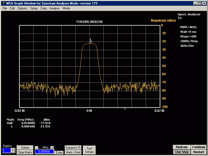
In this plot, the magnitude is indicating -23.67 dBm, with no input to the MSA. It would take an input signal of -23.67 dBm to duplicate this Response. Assuming Mixer 1 loss is -6.5 dB, and with an input signal of -23.67 dBm, the R Port output level would be at -30.17 dBm. Assuming the PLO 1 level at the Mixer 1 L Port is +7 dBm, then the L to R Port isolation of Mixer 1 would be: -30.17 dBm - (+)7 dBm = -37.17 dB. The Minicircuits spec calls for -37.5 dB isolation at this frequency, so this is right on target. If we used a "perfect" mixer that had infinite port to port isolation, the Zero Response would not exist.
This Zero Response will interfere with any input Signal of Interest that is close to the bandwidth of the Final Resolution Filter. Interference bandwidth includes frequencies outside of the 3 dB points. In the above plot, it would be obvious that an input signal at 1 KHz could not be measured unless its level is much greater than -23.67 dBm. An input signal at 12 KHz could not be measured unless its level was much greater than the Zero Response of -78 dBm at this frequency. If the 12 KHz signal were at a level of -50 dBm, it could be accurately measured by the MSA. You may ask, what is this noisy level outside of the 3 dB points? It is Phase Noise generated within the MSA.
MSA Phase Noise Contribution to Signal Magnitude Measurements
Phase noise generated within the MSA will degrade Spectrum Analyzer performance. All active circuits create and contribute phase noise to a system. Some circuits are significant contributors, others are not. I will deal with the two significant contributors to MSA phase noise, PLO 1 and PLO 2. It is a goal to minimize PLO phase noise, and this is discussed in the PLO paragraphs. PLO 2 phase noise is about 6 dB less than PLO 1 phase noise, so its contribution is about .97 dB to the total phase noise. Most all of the noise seen in the plot is contributed by PLO 1.
We can calculate the "close-in" phase noise of the MSA by using the data in the Zero Response Plot. It can be determined by calculating the difference of signal level to noise level at a particular frequency away from the carrier and converting to a 1 Hertz bandwidth. In the plot, the maximum signal level is measured as -23.67 dBm. The close-in phase noise can be seen at approximately 4 KHz away from the center of the response. It looks to be about -80 dBm, but we will take another plot with a narrow Video bandwidth to obtain more accurate values.
Phase Noise Plot

This is the same "Zero Response", but taken with a frequency log scale to show the upper side-band phase noise from 100 Hz to 1 MHz. The carrier level is -23.18 dBm (marker L). Marker 2 is the lowest frequency that phase noise can be measured. It measures -79.253 dBm at 4.365 KHz. The calculated phase noise (in a 1 Hertz bandwidth) can be determined by the formula:
Phase Noise (in a 1 Hz bandwidth) = noise power - Carrier power - 10 log BW (of Resolution filter).
PN = -79.253 dBm - (-23.18 dBm) - 10 log 3800/1Hz
PN = -79.253 dBm + 23.18 dBm - 35.798 dB = -91.871 dBc/Hz
This is the upper side-band phase noise at 4.365 KHz from the carrier. The lower side-band phase noise is assumed to be the same (and it really is).
This noise power of -91.871 dBc/Hz is the total combined noise power of PLO 1 and PLO 2. By design, the phase noise of PLO 2 is about 6 dB less than the noise power of PLO 1 (-6 dB is 25.11 %). The total noise power, Pt = P1 + P2, or Pt = P1 + .2511*P1, or Pt = 1.2511*P1.
Therefore, PLO 1 contributes 79.92 % of the total noise power and PLO 2 contributes 20.08 % of the total noise power. The actual phase noise of PLO 1 is -92.84 dBm/Hz, and PLO 2 is -98.84 dBm/Hz. The difference of the total measured phase noise of -91.87 dBm and the actual phase noise of PLO1 (-92.84 dBm) is .97 dB.
The calculated total phase noise at 10 KHz is -90.639 dBc/Hz, and at 100 KHz it is -108.783 dBc/Hz. The phase noise within 4 KHz of the carrier cannot be measured, due to the bandwidth limitation of the Resolution Filter (4 KHz). A much narrower Resolution Filter would be needed for very close-in phase noise measurements.
You may ask, what is the "hump" that is significant at marker 4. This is the loop bandwidth response for PLL 1. It is determined by the loop filter in PLO 1. It is sometimes called the "shoulder" or "knee" response. The loop response of PLO 2 cannot be seen because it is masked by the phase noise of PLO 1. The total PLO phase noise of the MSA becomes negligible at 400 KHz. This is where the noise of other circuits are predominant, and determine the input Noise Floor of the MSA. This means that MSA magnitude measurements will be most accurate at any frequency greater than 400 KHz. Input frequencies below 400 KHz will be measured by the MSA but accuracy will be degraded due to PLO phase noise contribution. However, any input signal that is greater than about 10 dB above the MSA phase noise level will be quite accurate. For example, a 100 KHz input signal that measures -60 dBm will be accurate, since the MSA phase noise level is about 15 dB less than the signal of interest.
MSA Phase Noise Contribution to Signal Phase Noise Measurements
The self-generated MSA phase noise will add directly to the phase noise of any input signal applied to the MSA. The MSA can measure the phase noise of an input Signal of Interest, but only if that Signal's phase noise is greater than the phase noise value of the MSA. For example, if the phase noise of a 10 MHz input signal is measured and calculated to be -108.783 dBc/Hz at 100 KHz away from the carrier, then its phase noise is better than indicated. The value of -108.783 dBc/Hz is the value of the MSA phase noise and "masks" the true phase noise of the signal. If the phase noise of that 10 MHz input signal is measured and calculated to be -88 dBc/Hz at 100 KHz away from the carrier, then its calculated phase noise is accurate. The contributed MSA phase noise is too low to degrade the measurement.
MSA phase noise is at its minimum at low frequencies, and increases at higher frequencies. For example, PLO 1 phase noise will increase by about 6 dB when the MSA is operated near 1000 MHz.
Hint: I suggest you duplicate the Phase Noise Plot in your MSA, print it out, and glue it to your work bench. You can quickly refer to the plot and determine if your input signal measurements are being affected by the internal phase noise of the MSA.
I will be the first to admit that there are many commercial spectrum analyzers with much better Phase Noise. But, if anyone can find a home brew, 1000 MHz SA with better phase noise, let me know.
PLO Phase Noise, General
There are a number of factors that determine the amount of phase noise that is created in a PLO. Frequency of operation, VCO noise, Reference noise, power supply noise, op. amp. noise, resistor noise, I.C. noise, the list is extensive and becomes a mathmatic nightmare. The bottom line is to have a PLO with a minimum amount of phase noise. Close-in phase noise of a PLO is mainly determined by the selection of PLL type, internal phase detector frequency, and frequency of VCO. Further-out phase noise is determined by the loop filter bandwidth.
To predict the close-in phase noise of a PLL :
Phase Noise (dBc/1 Hz bandwidth) = (1 Hz Normalized Phase Noise Floor of I.C.) + 10 log (phase detector frequency of PLL/1Hz) + 20 log (VCO frequency/phase detector frequency of PLL)
Using the values of PLO 1:
PN = -210 dBc/Hz + 10 log .972 MHz/1Hz + 20 log (1013.3 MHz/.972 MHz)
where -210 dBc/Hz is the 1 Hz Normalized Phase Noise Floor of the LMX 2326 (National Semi, spec)
where .972 MHz is the operating frequency of the internal phase/frequency detector of PLL 1,
where 1013.3 MHz is the operating frequency of VCO 1
PN = -210 dBc/Hz + 59.88 dB+ 60.36 dB= -89.76 dBc/Hz
This is the TOTAL close-in side-band noise in a 1 Hz bandwidth. Noise contributed by the loop filter components and the VCO will degrade this value farther from the carrier. Single side-band phase noise is half that. Example: -89.76 dBc/Hz - 3 dB = -92.76 dBc/Hz. This prediction is very close to the actual measurement of PLO 1 in the previous paragraphs (-92.841 dBc/Hz).
Using the maximum allowable phase detector frequency (PDF) for the PLL will result in lowest phase noise. Maximum PDF is specified by the PLL I.C. The SLIM PLO-1 and SLIM PLO-2 use the LMX2326 (National Semi) or the ADF4112 (Analog Devices).
PLO 1 using SLIM-PLO-1
PLO 1 is the "Tunable Local Oscillator" that controls the frequency of the MSA. A fully configured SLIM-PLO-1 has two active outputs, J2 and J3, both with a power level designed to be +10 dBm. One is used to drive the Mixer 1 module for the Basic MSA and the other is used to drive the Mixer 4 module, for the VNA extension. Nominal frequency of operation is from 950 MHz to 2030 MHz. The upper frequency limit can be extended by increasing the +20 volt source. The maximum voltage limit is determined by the specifications of the VCO's tuning voltage. The Minicircuits ROS-2150VW tuning voltage is rated at +25 volts, but +30 volts will not harm it.
I have had a few users report that the output levels may be lower than the expected +10 dBm. For more information, see the Engineering Notice, 10-25-08 on the web page, SLIM-PLO-1. I need not duplicate that information here. Even with a lower level, the MSA will function, but with lower total MSA gain. I would be concerned if a PLO output level is less than +6.5 dBm.
The loop filter design for PLO 1 is a compromise between phase noise and lock time. We could decrease the bandwidth of the loop filter to increase lock time and decrease phase noise, but that would slow the sweep speed of the MSA. Replacing the LMX 2326 with an Analog Devices ADF 4112 will improve phase noise performance a little. The op amp I.C. (LT 1677) was about the best choice at the time (Aug-07). There may be better ones on the market as time progresses.
A quick test to verify that PLO 1 is operating and locked at 1013.3 MHz, the voltage on the VCO control line should be +2.55 volts +/- 10%. (MSA is tuned to 0 MHz)
PLO 3 using SLIM-PLO-1
PLO 3 is the "Tunable Local Oscillator" that controls the frequency of the Tracking Generator and VNA. A fully configured SLIM-PLO-1 has two active outputs, J2 and J3, both with a power level designed to be +10 dBm. One is used to drive the Mixer 3 module for the Tracking Generator and the other is used to drive the Mixer 4 module, for the VNA extension.
PLO 3 is identical PLO 1, so its analysis is identical to PLO 1. Its phase noise is evident when the Tracking Generator output is used as a Signal Generator. It is not so evident when the Tracking Generator is used as the Signal Source for VNA operation. This is because the MSA is always tuned to the center frequency of the Trackng Generator signal (center of carrier) and the side-band phase noise is never measured.
A quick test to verify that PLO 3 is operating and locked at 1024 MHz, the voltage on the VCO control line should be +2.64 volts +/- 10%. (Signal Generator is commanded to 0 MHz)
PLO 2 using SLIM-PLO-2
PLO 2 is the "Fixed Local Oscillator" for both the Spectrum Analyzer and the Tracking Generator. A fully configured SLIM-PLO-2 has two active outputs, J2 and J3, both with a power level designed to be +10 dBm. The Basic MSA requires only one output from the PLO 2, used as the LO drive for Mixer 2. The other output is used to provide the 1024 MHz source for Mixer 3, the Tracking Generator Output.
PLO 2 phase noise is calculated the same way as PLO 1. Its PLL's phase/frequency detector is operating at a higher speed (4 MHz, compared to .97 MHz of PLL 1). This produces less phase noise. It could be operated at 8 MHz to produce even less phase noise.
A quick test to verify that PLO 2 is operating and locked at 1024 MHz, the voltage on the VCO control line should be +3.2 volts +/- 10%.
DDS 1, using SLIM-DDS-107
The MSA configurations require only one output from DDS 1, the output from the Squaring Buffer, J4. It is used as the reference clock input to J1 of PLO 1. The output frequency is commanded from 10.69 MHz to 10.71 MHz in about 15 milliHertz increments. The output level is 3 volts peak to peak into 50 ohms. The combination of DDS 1 and PLO 1 creates a Hybrid Synthesizer that will operate from 950 MHz to 2030 MHz.
The "spare out" at J3 (DDS B) is an unbuffered output of the DDS I.C. It can be used as a frequency source for other purposes. It can be commanded to any frequency from 0 Hertz to 32 MHz in about 15 milliHertz increments. It has an output level of approximately -8 dBm. The signal will also contain alias frequencies and harmonics that reach well into the GHz region.
The 64 MHz Master Oscillator is used as a Clock Source for the DDS and is input on J1. J1 has the capability to present a 50 ohm load to the Master Oscillator, but it is recommended that it not be used. This will allow a full 5 volt peak to peak signal to drive the DDS I.C. The return reflection of the clock caused by the unterminated line will be absorbed back at the Master Oscillator Module. This may seem like a poor design, but it results in an extremely low phase noise output of the DDS.
DDS 3, using SLIM-DDS-107
The MSA configuration with the Tracking Generator requires only one output from DDS 3, the output from the Squaring Buffer, J4. It is used as the reference clock input to J1 of PLO 3. The output frequency is commanded from 10.69 MHz to 10.71 MHz in about 15 milliHertz increments. The output level is 3 volts peak to peak into 50 ohms. The combination of DDS 3 and PLO 3 creates a Hybrid Synthesizer that will operate from 950 MHz to 2030 MHz. DDS 3 and DDS 1 are identical.
Mixer 2 using SLIM-MXR-2
The first I.F. of 1013.3 MHz is mixed with 1024 MHz from LO 2. The expected output frequency at port I is 10.7 MHz. However, there will be other frequencies, such as the additive mixing component, R+L = 2037.3 Mhz. Some signal at the L port will feed through to the I port, and so will some signal from the R port. Mixer 2 uses a low pass filter/diplexer, with crossover at 33 MHz. This allows the 10.7 MHz I.F. to pass to J2, while preventing the high frequency components from leaving J2 and getting to the MSA's I.F. Amplifier.
The internal 2.5 dB attenuator in the L Port path improves the conversion effeciency and port to port isolation of the ADE-11X. The LO power level applied to Mixer 2 is +10 dBm (from PLO 2) and the attenuator drops it to 7.5 dBm, the level for the ADE-11X's L port.
I.F. Amplifier using SLIM-IFA-33
The SLIM-IFA-33 has two independent amplifiers with an operating bandwidth of 3 to30 MHz. The output of one (J4) is connected to the input of the other (J1) with a short piece of coaxial cable. This gives a total gain of 40 dB. Saturated output is +14 dBm.
Due to the gain of the amplifiers, the amount of generated wide band noise is substantial. By formula:
-174 dBm + 3 dB(noise figure) + 40 dB(gian) + 10 log 27 MHz(BW) = -56.7 dBm
Some form of bandwidth limitation filter is required between the amplifier output and the input to the Log Detector module. The Resolution Bandwidth filter will accomplish this requirement.
Resolution Bandwidth Filter, aka. Final Xtal Filter
The Final Xtal Filter determines the Resolution Bandwidth of the MSA. Steep slopes and out of band rejection is a must for good selectivity. A secondary and not-so-obvious function of the Resolution Filter is to limit the wide band noise that is created by the previous I.F. Amplifier.
The MSA Block Diagram does not specify a particular Final Xtal Filter for this position. The MSA software has provision for up to 4 Resolution Bandwidth Paths. The filters can vary in bandwidth, insertion loss, and even center frequency. The stipulation is that the total bandwidth of the filters must not exceed the bandwidth of the Coaxial Cavity Filter.
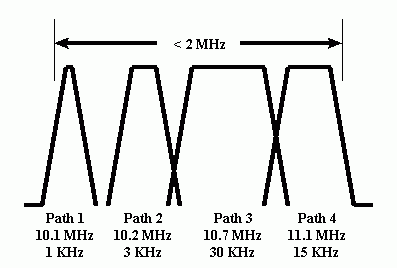
The frequency distance from the lower 3 dB point of the lowest frequency filter to the upper 3 dB point of the highest frequency filter must be less than the total 3 dB bandwidth of the Cavity Filter (nominally, 2 MHz). The Paths do not have to be in frequency order. The Cavity Filter Center Frequency will then be tuned to a frequency that is determined by the center frequency of the Filter Paths. In the above example drawing, the 4 final filters occupy a frequency range from 10.095 MHz to 11.1075 MHz. The center frequency of the Filter Paths is 10.60125 MHz. With PLO 2 operating at 1024 MHz, the average center frequency of the First I.F. is 1013.3988 MHz. This is where you would want the center frequency of the Coaxial Cavity Filter. This is so close to the design frequency of 1013.3 MHz, it is not worth re-tuning. However, other Final Path Filter choices can move this average frequency and re-tuning the cavity filter would be advisable.
Coaxial Cavity Filter. Cavity Filter Construction Page
The primary path for the First I.F. (1013.3 MHz) is from Mixer 1 through the Coaxial Cavity Filter, and then to Mixer 2. The main purpose of this filter is to attenuate the MSA input image frequency, which is at 1034.7 MHz. Insertion loss is not important, but a large loss may indicate a failure. Since this filter is home-brew, insertion loss can be anywhere between -3 dB and -8 dB. The rejection ratio at 1034.7 MHz should be at least -70 dBc for minimal operation of the MSA. A -100 dBc rejection ratio is typical, and will result in execllent MSA operation. Greater than -112 dBc can be attained by tuning the filter a little lower in frequency and allowing the First I.F. of 1013.3 MHz to occupy the upper region of the filter bandpass. See the paragraph on Resolution Bandwidth Filter for more information on tuning the Coaxial Cavity Filter.
The 3 dB bandwidth is approximately 2.0 Mhz, but is dependent on the interstage coupling. Coupling is determined by the position of the input, output, and interstage hairpins during construction. The common trend is: Hairpins that are closer to the cavity walls results in undercoupling, narrower bandwidth, and higher insertion loss. Hairpins that are farther from the cavity walls results in overcoupling, wider bandwidth, and lower insertion loss.
Log Detector using SLIM-LD-8306
The Log Detector Module is the mechanism for converting RF power to a dc voltage. The SLIM-LD-8306 has a broadband (160 MHz) input transformer. Be aware that this log detector is very responsive to wide band frequencies, and noise. For maximum MSA sensivity, the Log Det Module must be preceeded by a filter that will limit the input noise to less than -90 dBm. In the MSA, this function is performed by the Final Xtal Filter. A 30 KHz bandwidth filter with an insertion loss of -3.8 dB will limit the noise to -90dBm. Wider bandwidth filters can be used, but they will allow more noise to desensitize the Log Detector, resulting in a higher MSA noise floor.
The SLIM-LD-8306 has two outputs:
The Mag(nitude) Volts Output at J2 is a DC voltage, where its level is relative to the amount of input power to the module. The output is approximately .3 volts to 2.3 volts for a power input (Log Det input) of -90 dBm to +10 dBm. The converion factor is 20 millivolts per dB. This output is passed to the Analog to Digital Converter for use by the computer.
The second output, Lim(ited) IF Out on J3, is not used in the Basic MSA. It is a square wave of the input at J1. It is used when the MSA is expanded to the MSA/VNA configuration. If you plan not to use this output, do not install R4-R6, and C12. This will disable the limiter section of the I.C. The peak to peak level of this signal is controlled by the value of R6. The level is held to a minimal voltage that can be processed by the Phase Detector Module. A large level has the possibility to cause instability of operation (self-oscillation). I have been told that R6 can be decreased to 150 ohms without instability. I have not verified this.
Another deviation from design is to add a small capacitor (10-20 pfd) across the outputs of the AD8306 (U2, pin 12 to pin 13). This decreases the output bandwidth (noise) and may decrease the potential of instability if R6 is decreased in value. I have tried a 20 pfd cap and the lower output noise extended the usable range of the Phase Detector by a few dB. This is an area the experimenter may like to play with.
After much testing of the Log Detector, I have concluded that its input noise floor is dependent on its operating temperature. If your MSA will use a Final Xtal Filter with a bandwidth of less than 15 KHz, I suggest locating this module in the coolest spot in your assembly. Under a fan or next to a wall, away from excess heat. You will not see any difference when using wider bandwidths.
For the adventurous builder, there is an experimental modification to the Log Detector to improve its dynamic range. It is described on the bottom of the page at SLIM-LD-8306 .
I previously stated, "The Log Detector Module is the mechanism for converting RF power to a dc voltage." This statement is true, but it should be put into proper context. The module uses an Analog Devices, AD 8306 Logrithmic Detector integrated circuit. It is actually a voltage converting device, not a power converting device. Its input resistance is approximately 1 K ohms. A transformer is placed between the input of the module and the I.C. to transform the I.C. input resistance of 1 K ohms to an input resistance of the module of 50 ohms. The transformer has a 1:4 turns ratio which creates a 1:16 impedance ratio. The actual output impedance of the transformer is 16 x 50 = 800 ohms. Obviously, this 800 ohms does not present the proper impedance of 1 K ohms that the I.C. wants to see. Therefore, a 4.02 K ohm resistor is placed on the 1 K ohm input of the I.C. to create a total resistance of 801 ohms. The resistance matching reduces the effeciency of the power transformation, but this is easier than winding a custom transformer.
The specified Minicircuits transformer allows an input frequency range of .2 MHz to 160 MHz. The MSA's I.F. is typically 10.7 MHz. I could have designed the input transformation (50 ohms to 1K ohms) as an L/C circuit rather than a transformer. This would improve effeciency but would also confine the input frequency to 10.7 MHz. Since the SLIM-LD-8306 is intended to be a general purpose logrithmic detector, I did not want to limit the module to any specific frequency.
The Dynamic Range of the Log Detector determines the maximum dynamic range of the MSA. Analog Devices specifies the dynamic range of the AD 8306 to be 100 dB., with an input voltage range of -91 dBv to +9 dBv (28.18 microvolts to 2.818 volts). Due to the 1:4 voltage transformation, the voltage range on the 50 ohm input of the Module is 7.045 microvolts to .7045 volts. This equates to -90 dBm to +10 dBm.
A to D Converter, using either a 12 or 16 Bit Serial A to D Converter:
The A to D Converter has two A/D circuits, but only one is used in the Basic MSA. The other is used when the MSA is expanded to VNA operation. For the Basic MSA. the "PHA VOLTS" section can be deleted. That would be U3 and all of it's supporting components. This module has no adjustment potentiometer for calibration. With 12 or 16 bit resolution, adjustment is not necessary for the MSA.
For VNA operation, there is an optional configuration. This option changes the way power is supplied to the to the A to D Converter. Instead of the Control Board supplying +10 volts to the A to D Converter, the Phase Detector Module will supply a regulated +5 volts to the A to D Converter. This option will improve the Phase Measurement accuracy of the VA. For this option, the SLIM-ADC-12 or SLIM-ADC-16 is modified. The 5 volt regulator, U1 is removed and bypassed with a wire. This allows both the PDM and ADC to share the same 5 volt source as a common reference.
16 Bit Serial A to D Converter using SLIM-ADC-16
The "MAG VOLTS" input is connected back to the Log Detector's Magnitude output. J1 will accept an input range of 0 volts to +5 volts, but the Log Det. output voltage is expected to range only from +0.4 volts to +2.4 volts (its maximum 100 dB range). This 16 Bit AtoD will convert +0.4 volts to a bit value of "5243". The bit value of +2.4 volts is "31457". The dynamic bit range is 31457 - 5243 = 26214 bits. Therefore, the conversion factor for the MSA's combination of Log Det and 16 Bit AtoD Converter is: 100 dB/26214 bits = .0038 dB per bit. This determines the Magnitude Resolution of the MSA.
The "PHA VOLTS" (J2) is configured for an input dynamic range of 0 volts to +5 volts, the range expected from the Phase Detector Module. This 5 volt range equates to 360 degrees. Therefore, the resolution of the SLIM-ADC-16 is 360/65536 = .0055 degrees per bit. This determines the Phase Resolution of the MSA.
12 Bit Serial A to D Converter using SLIM-ADC-12
The J1 (MAG VOLTS) section is configured for an input dynamic range of 0 volts to +2.8 volts. The "MAG VOLTS" input is connected back to the Log Detector's Magnitude output, which is expected to range from +0.4 volts to +2.4 volts, (the maximum 100 dB range of the Log Det). This 12 Bit AtoD will convert +0.4 volts to a bit value of "585". The bit value of +2.4 volts is "3511". The dynamic bit range is 3511 - 585 = 2926 bits. Therefore, the conversion factor for the MSA's combination of Log Det and 12 Bit AtoD Converter is: 100 dB/2926 bits = .034 dB per bit. This determines the Magnitude Resolution of the MSA.
The "PHA VOLTS" (J2) section was originally designed for an input dynamic range of +1 volt to +4 volts, but should have been modified for the range of 0 volts to +5 volts, the expected input from the Phase Detector Module, J3. The resolution is 360 deg/4095 bits = .0879 degrees per bit. This determines the Phase Resolution of the MSA.
Mixer 3 using SLIM-MXR-3
MXR-3 is used only when the Tracking Generator is added to the Basic MSA. MXR-3 output is the difference frequency of the inputs, PLO 3 and PLO 2. The primary output frequency range is 0 to 1000 MHz. The output level is approximately -10 dBm with an expected ripple of 2 dB.
Both input paths have internal attenuators, a 2.5 dB attenuator in the L port path and a 14 dB attenuator in the R port path. These localized attenuators improve the conversion effeciency and port to port isolation of the ADE-11X. The PLO 3 power level applied to Mixer 3 is +10 dBm and the attenuator drops it to 7.5 dBm, the level for the ADE-11X's L port. The 1024 MHz power level applied to Mixer 3 is +10 dBm (from PLO 2) and the attenuator drops it to -4 dBm, the level for the ADE-11X's R port.
There is one modification (Rev A) that is on the schematic and parts list, but needs mentioning here. The R Port of Mixer 3 is operating at a fixed frequency of 1024 MHz. The ADE-11X R port impedance is not exactly 50 ohms. Matching the mixer's R port to the internal 14 dB attenuator can be greatly improved by adding a 2.0 or 2.2 pF chip capacitor in the C9 position. This is on the ADE-11X, pin 3 to ground. This improves the port to port isolation of the mixer and reduces cross-talk interference within the MSA. This is not a perfect matching arrangement, and the experimentor could "play" in this area for improvement.
Mixer 4 using SLIM-MXR-4
MXR-4 is used when the MSA/TG is extended into a VNA. MXR-4 output is 10.7 MHz when the Tracking Generator is activated. The output level is approximately -10 dBm.
Note here, that SLIM-MXR-4 has been revised to Rev A. This revision adds an internal 2.5 dB attenuator in the L port path and a 14 dB attenuator in the R port path. These localized attenuators improve the conversion effeciency and port to port isolation of the ADE-11X. The LO power level applied to Mixer 3 is +10 dBm (from PLO 1) and the attenuator drops it to 7.5 dBm, the level for the ADE-11X's L port. The R power level applied to Mixer 3 is +10 dBm (from PLO 3) and the attenuator drops it to -4 dBm, the level for the ADE-11X's R port.
PDM, Phase Detector Module, using SLIM-PDM
The PDM is used only when expanding the MSA/TG into the VNA. This module operates at 10.7 MHz and has squaring circuits within it. Consequently, it is a potential radiator of harmonic noise. It is extremely important that this module be well shielded. When the VNA is not operating, this module is still actively amplifying noise or real signals created by the Log Detector and Mixer 4. "Funnies" in the MSA spectrum could be attributed to a "radiating" PDM. I have tested some of these harmonics well into the GHz region.
If the PDM module is suppliying + 5 volts to the Analog to Digital Converter module, FB2 is installed between U5-8 and P2-2. On the schematic, this is the FB2 position. Also, the FBx position is populated with another ferrite bead, a zero ohm resistor, or a jumper wire. I recommend a ferrite bead. This optional topology is recommended for the MSA/VNA. It improves the Phase Measurement accuracy, since both the PDM and A to D are using the same +5v reference voltage.
Master Oscillator using SLIM-MO-64
The SLIM-MO-64 uses a 64 MHz crystal oscillator and has three buffered outputs. Two are used in the Basic MSA. The third is used for the Tracking Generator addition. The users of the Master Oscillator are DDS 1, PLO 2, and DDS 3. 50 ohm coax is used to connect the outputs to the users, but the users are terminated in a high impedance load. The signal will reflect back to the output of the Master Oscillator module and be absorbed by the buffer amplifier and 33 ohm driving resistor. This may seem a like poor design but it is valid. It improves the noise performance of the users. It also minimizes the power consumption of the Master Oscillator module.
The actual frequency will not be exactly 64.000 MHz. However, it will likely be within 1 KHz. It does not matter. The MSA software will compensate for any frequency. The main concern for the Master Oscillator is frequency drift. This will be determined by the temperature of the 64 MHz oscillator.
The Master Oscillator will draw approximately 50 ma of current and consume 250 mw of power. This may not seem like much, but will produce heat. The heat produced will cause the 64 MHz oscillator to change in frequency. At some point, heat stabilization will occur and frequency drift will halt. Normally, this will take about 30 minutes, but there are other factors that contribute to this time. If there is no venting in the enclosure, stabilization may take hours or perhaps, may never reach stabilization. An internal fan within the MSA enclosure will speed the stabilization time.
Other Stuff
Fan Addition:
I had previously stated that it was not a good idea to use a fan inside the MSA for cooling. The reason is vibration. There are several components in the MSA that are sensitive to vibration. The most critical are the Master Oscillator and Final Crystal Filter, due to their piezo characteristics. Oddly enough, coaxial cables also have piezo characteristics.
I am going to retract my concerns a bit. I have tested the Verification MSA with a muffin fan on the bottom cover. It is pointed directly up, at the bottoms of the Log Detector module and Master Oscillator module. The muffin fan is a 2.5 inch, 24 volt, rated at 90 ma. I am running it off the +13.6 volt input line, and it is drawing 40 ma. I cut a 2.5 inch hole in the top and bottom covers for the air flow. With it "half blowing" it is keeping the MSA, cool as a cucumber.
I have tested for vibration effects in MSA Mode and VNA Mode and see absolutely no ill effects. Therefore, a really "quiet" fan, is acceptable. Muffin fans tend to inject a large amount of "hash" on its power lines. It is important that the lines be well filtered. I suggest installing a resistor/capacitor low pass filter network on its supply line.
Updated 10-1-15.
You came to this page because:
A. You are interested in the technical aspects of the MSA.
B. Your MSA is not functioning properly and need some troubleshooting guidance.
C. You are learning about RF circuits and crave for more information.
D. You are an RF guru and want to critique my design. OK, that's fine, I'm not perfect and I make mistakes. E-mail me and offer suggested improvements.
E. You pushed the wrong button. You think "RF" means Redwood Fence. Use your browser's "Back" button and leave before your brain turns to mush.
This Technical Analysis of the MSA is for those who are interested in the inner workings of the MSA. It can be helpful for troubleshooting the MSA. This page will be divided into sections:
System Description
Block Diagram
The Basic MSA, the Spectrum Analyzer
The MSA with Tracking Generator
The Vector Network Analyzer
System Analysis
MSA Gain
Input Sensitivity
Maximum Input Power Level
Input Dynamic Range
MSA Input Noise Floor
Other Factors Affecting Analysis
Module Analysis
Local Oscillator Output Levels and Mixer Drive
Control Board using SLIM-CB-NV
Mixer 1, the Input Stage of the MSA
Mixer 1, Isolation
MSA Phase Noise Contribution to Signal Magnitude Measurements
MSA Phase Noise Contribution to Signal Phase Noise Measurements
PLO Phase Noise, General
PLO 1 using SLIM-PLO-1
PLO 3 using SLIM-PLO-1
PLO 2 using SLIM-PLO-2
DDS 1, using SLIM-DDS-107
DDS 3, using SLIM-DDS-107
Mixer 2 using SLIM-MXR-2
I.F. Amplifier using SLIM-IFA-33
Resolution Bandwidth Filter, aka. Final Xtal Filter
Coaxial Cavity Filter
Log Detector using SLIM-LD-8306
A to D Converter, using either a 12 or 16 Bit Serial A to D Converter:
16 Bit Serial A to D Converter using SLIM-ADC-16
12 Bit Serial A to D Converter using SLIM-ADC-12
Mixer 3 using SLIM-MXR-3
Mixer 4 using SLIM-MXR-4
PDM, Phase Detector Module, using SLIM-PDM
Master Oscillator using SLIM-MO-64
Other Stuff
Fan Addition
Spurious, Interference, and other Weird Stuff in the MSA
Spurious Defined
Spur Creation in the Basic Spectrum Analyzer
Spur Creation in the Spectrum Analyzer plus Tracking Generator
Spur Creation in the VNA
Known Spurious Signals and Interference
PLO 3 - PLO 1 Spurious
PLO 3 - PLO 2 Spurious
PLO 3 Harmonic Interference
System Description
Block Diagram
There are three MSA configurations. The Basic MSA, the MSA with Tracking Generator addition, and the MSA with VNA extension. This is the block diagram of the MSA with VNA extension.
You will notice that several items within the block diagram do not have committed connections. This is because the MSA can have several bands of operation, and the interconnections depend upon the band of operation. They will be explained in the following paragraphs.
The Basic MSA, the Spectrum Analyzer
Common Configuration for all Bands: A dual conversion topology is used to minimize internally generated spurious. A 10.7 MHz Final I.F. is chosen to take advantage of commercially available filters. The magnitude detector is a logrithmic detector with 100 dB of dynamic range, driving a 16 bit Analog to Digital Converter. There are two local oscillators, LO 1 driving Mixer 1, and LO 2 driving Mixer 2. LO 1 is comprised of a Phase Locked Oscillator (PLO 1) and a Direct Digital Synthesizer (DDS 1), arranged as a hybrid synthesizer. LO 2 is a Phase Locked Oscillator (PLO 2), commanded to a fixed frequency of 1024 MHz. A 64 MHz Master Oscillator is used as the reference. A Control Board interfaces the MSA to the home computer.
1G Band of Operation: The MSA frequency range is from 0 to 1000 MHz and the input is J2 of Mixer 1. PLO 1 is variable, from 1013.3 MHz to 2013.3 MHz, and will high-side mix with the input frequency. The converted output at J3 of Mixer 1 is 1013.3 MHz, and is passed to the Coaxial Cavity Filter for image rejection. Its output is mixed with PLO 2, a fixed frequency of 1024 MHz. to produce the Final I.F. of 10.7 MHz. The final I.F. is low pass filtered within Mixer 2 and is present at J2. The final IF is passed to J3 of the I.F. Amplifier, amplified, and passed to a user selected, Final Xtal Filter. This filter determines the Resolution Bandwidth of the MSA. The magnitude of the signal is converted to a relative voltage by the Log Detector and processed by the Analog to Digital Converter. The digital signal is passed through the Control Board to the home computer for software processing.
3G Band of Operation: The MSA frequency range is from 2000 to 3000 MHz and the input is J2 of Mixer 1. PLO 1 is variable, from 986.7 MHz to 1986.7 MHz, and will low-side mix with the input frequency. The converted output at J3 of Mixer 1 is 1013.3 MHz, and is passed to the Coaxial Cavity Filter for image rejection. Its output is mixed with PLO 2, a fixed frequency of 1024 MHz. to produce the Final I.F. of 10.7 MHz.
The J2 input port of Mixer 1 has degraded performance for input frequencies above 1000 MHz. Although the 3G Band of the MSA is responsive with this configuration, it is better to reverse the input/outport ports of Mixer 1. The MSA input would become J3 of Mixer 1 and the 1st I.F. would exit J2.
2G Band of Operation: The MSA frequency range is from 1000 to 2000 MHz. With a physical change to the path topology, the MSA is changed to a single conversion topology. PLO 1 is variable, from 1010.7 MHz to 2010.7 MHz, and will high-side mix with the input frequency. The converted output at J3 of Mixer 1 is 10.7 MHz, and is passed to the 2G Low Pass Filter. Its output is passed to J3 of the I.F. Amplifier, amplified, and passed to a user selected, Final Xtal Filter. The Coaxial Cavity Filter and Mixer 2 are not used for 2G Band operation.
Again, the J2 input port of Mixer 1 has degraded performance for input frequencies above 1000 MHz. Although the 2G Band is responsive with this configuration, it is better to reverse the input/outport ports of Mixer 1. The MSA input would become J3 of Mixer 1 and the Final I.F. would exit J2.
This single conversion scheme has no image rejection. That is, Mixer 1 will act as a low-side mixer and will produce the same 10.7 MHz conversion frequency for input frequencies of 1021.4 MHz to 2021.4 MHz. This is because input signals can be either 10.7 MHz above LO 1 or 10.7 MHz below LO 1.
The MSA with Tracking Generator
The Tracking Generator is comprised of PLO 2, PLO 3, and Mixer 3. PLO2 (1024 MHz) and PLO 3 (1024 MHz to 2124 MHz) are combined in Mixer 3 to produce the TG Output. For 1G and 3G Band operation, J2 of PLO 3 is connected to J1 of Mixer 3. The TG output is at J2 of Mixer 3.
Subtractive mixing (PLO3-PLO2) produces the TG output range from 0 MHz to 1000 MHz (1G Band). Additive mixing (PLO3+PLO2) produces the TG output range from 2000 MHz to 3000 MHz (3G Band). Also, there are plenty of harmonic products created by Mixer 3. These are too numerous to list and the power levels are uncertain. These multiple TG output signals can be of good use, or they can be detremental. Some form of external filtering must be added to the TG output to attenuate unwanted frequencies. The formula for the Tracking (or Signal) Generator output frequency is TG = Q*PLO 3 + M*PLO 2, where Q and M can be any positive or negative integer number, including zero.
During 2G Band operation, the same Mixer 3 configuration will produce a TG output from 1000 MHz to 2000 MHz. However, the power level will be quite low since there is no "mixing" within Mixer 3. The TG signal is the mixer isolation leakage of PLO 3. It is better to re-configure and use the J2 output of PLO 3 for the Tracking Generator. It will have a power level of approximately +10 dBm.
The Vector Network Analyzer
The VNA extension is comprised of PLO 1, PLO 3, Mixer 4 and the Phase Detector Module (PDM). Mixer 4 output is the difference frequency of PLO 1 and PLO 3. The difference frequency between PLO 1 and PLO 3 will always be the same as the Final I.F. frequency (10.7 MHz). Mixer 4 output is the "Phase Reference" supplied to the PDM. The power level is approximately -10 dBm. The second input of the PDM is supplied by the Limiter section of the Log Detector Module. This is the limited Final I.F. and is the "Phase Signal" that is measured, relative to the Phase Reference. It is a square wave with a level of approximately 30 mvpp. The output of the PDM (Phase Volts) is a DC voltage that is proportional to the differential phase of its two input signals. The Phase Volts is converted to a digital format by the Analog to Digital Converter and passed through the Control Board to the Computer for processing.
System Analysis
MSA Gain
First, approximate gains and losses in the SLIM MSA. Each mixer has -6.5 dB of loss. The coaxial cavity filter has -7 dB of loss. The dual I.F. Amplifier has +40 dB of gain. The loss of the Final Xtal Filter (Resolution Bandwidth Filter) can vary, but for now, assume it has -4 dB loss and a bandwidth of 2.2 KHz. The total MSA gain (from MSA input to Log Detector Module) = -6.5dB -7dB -6.5dB +40dB -4dB = +16 dB. This is a nominal value. Any deviation of the previously mentioned components would change this gain figure. Probably the biggest contributor to gain difference can be attributed to the coaxial cavity filter. Its insertion loss is dependent on its construction and tuning, and can range anywhere between -3 dB to -8 dB. The mixer loss of -6.5 dB is dependent on its LO drive level. Lower drive level will result in greater mixer loss, but it is not dB for dB. Lowering the drive level by 3 dB may only degrade mixer loss by 1 dB. If Mixer 1 has internal attenuation in its input path, the total MSA gain will be reduced by the amount of the attenuator.
Input Sensitivity, Minimum Signal Input Power Level
For the MSA, I define sensitivity as the minimum input signal power that can be measured and quantified. MSA sensitivity is mostly dependent on the sensitivity of the SLIM Log Detector, but the Resolution Bandwidth Filter will play a significant role in determining sensitivity. Its role will be explained in the paragraph "MSA Input Noise Floor". For the following analysis, assume the RBWF is 2.2 KHz.
For Magnitude, this is the input power level that causes the graphed noise floor to increase. Analog Devices specifies the input noise floor of the AD8306 to be -91 dBv (28.18 microvolts). Due to the 1:4 voltage transformation within the Log Detector Module, the input voltage at the 50 ohm input of the SLIM Log Detector Module is 7.045 microvolts (-90 dBm). Using the MSA Gain figure of 16 dB, the minimum signal level at the input to the MSA would be: -90 dBm - 16 dBm = -106 dBm.
For Phase, this is the input power level that causes the Limited RF output of the SLIM Log Detector to deviate more than 2 degrees. Analog Devices specifies this input to the AD8306 to be -73 dBv. This equates to -72 dBm input to the Log Detector Module. Using the MSA Gain figure of 16 dB, the minimum signal level at the input to the MSA would be: -72 dBm - 16 dBm = -88 dBm.
Maximum Input Power Level
There are three quantities to define here. One is the maximum input signal to the MSA without causing destruction. This level is the maximum input to Mixer 1 (ADE-11X) and is +17 dBm (50 mw).
The other two are the maximum input power levels that can be quantified as a Magnitude measurement or a Phase measurement. These levels are mostly dependent on the saturation level of the SLIM Log Detector.
For Magnitude, Analog Devices specifies the maximum input to the AD8306 I.C. to be +9 dBv (2.818 volts). Due to the 1:4 voltage transformation within the Log Detector Module, the input voltage at the 50 ohm input of the SLIM Log Detector Module is .7045 volts (+10 dBm). Using the MSA Gain figure of 16 dB, the maximum signal level at the input to the MSA would be -6 dBm.
For Phase, Analog Devices specifies the maximum input to the AD8306 to be -3 dBv, to preven phase distortion. This equates to -2 dBm input to the Log Detector Module. Using the MSA Gain figure of 16 dB, the maximum signal level at the input to the MSA would be -18 dBm.
Input Dynamic Range
The MSA Dynamic Range is the difference between minimum measurable input signal and the maximum measurable input signal.
For Spectrum Analyzer Mode, the minimum and maximum magnitude levels at the input to the MSA was analyzed be -106 dBm and -6 dBm. This would indicate that the Spectrum Analyzer Input Dynamic Range is 100 dB.
For VNA Mode, the minimum and maximum magnitude level to maintain a constant phase was analyzed be -88 dBm and -18 dBm. This would indicate that the VNA Input Dynamic Range is 70 dB.
However, the previous analysis uses the specifications of the AD8306 Log Detector. In reality, it will operate outside of its specifications and can be characterized. Characterization takes place during MSA Calibration.
MSA Input Noise Floor
The previous analysis for Power Levels and MSA Dynamic Range assumed that the noise floor of the MSA was determined by the Log Detector. This paragraph explains how the analysis is justified.
The Input Noise Floor of the MSA is determined by the self generated noise of all the circuits within the MSA. That is, it is assumed that there is no "real" signal entering the MSA to be measured by the Log Detector. This is a reality if the MSA is commanded to any frequency that does not create spurious signals. Spurs are explained near the end of this page. The devices, Mixer 1 and Mixer 2 do create noise, but their total level is below the physical noise floor of -174 dBm/sqrtHz (a 1 Hz bandwidth).
Therefore, the total noise created in the MSA is the combination of the two I.F. Amplifiers and the Log Detector. The first I.F. Amplifier has a noise figure of 3 dB and a gain of 20 dB. The broad-band noise generated by the first amplifier is = -174dBm +3dB(amp noise figure) +20dB(gain) = -151 dBm /sqrtHz. The second amplifier (20 dB gain) increases the noise to -131 dBm /sqrtHz. This output noise must pass through the Resolution Filter before it enters the Log Detector. The Filter will limit the bandwidth of the noise to the bandwidth of the Filter. The Filter will also reduce the noise by an amount equal to the insertion loss of the Filter. (Assume the bandwidth is 2.2 KHz, with -4 dB loss). The total noise at the input to the Log Det SLIM = -131 dBm /sqrtHz + 10logBW(2.2KHz) - 4dB(filter loss) = -131 +33.4 -4 = -101.6 dBm. This total noise value of -101.6 dBm is much lower than the input noise floor (-90 dBm) of the Log Detector. This means that the Log Detector is determining the noise floor and the previous assumption that the MSA Dynamic Range of 100 dB is valid.
If the 2.2 KHz Final Xtal Filter is replaced with a 15 KHz bandwidth filter, the total noise input to the Log Detector will increase. The total noise at the input to the Log Det will be: Total noise = -174dBm +3dB(amp noise figure) +20dB +20dB +10logBW(15KHz) -4dB(filt loss) = -174+3+40+41.8-4 = -93.2 dBm. This total noise level is 3.2 dB lower than the -90 dBm noise floor of the Log Detector. The Log Detector is still determining the noise floor and the MSA Dynamic Range of 100 dB is still valid.
The question becomes, what is the maximum bandwidth we can use for the Resolution Filter and not add noise.The maximum value of noise bandwidth that can be added between the amplifier output and the Log Detector input is (131-90) = 41 dB. Assuming a -4 dB Filter insertion loss, the noise power addition becomes 41+4 = 45 dB. Using a reverse calculation to the formula (10logBW=45), BW = 10^45/10 or 10^4.5 = 31,623 Hz. Therefore, a Resolution Bandpass Filter of 31.6 KHz is the widest Filter we can use and still maintain full Dynamic Range.
A Resolution Filter wider than 31.6 KHz will increase the total input noise to the Log Detector to a level higher than the self induced noise floor of the Log Detector, thus reducing the Dynamic Range. For example, using a 300 KHz Filter. The Total noise = -174dBm +3dB(amp noise figure) +20dB +20dB +10logBW(300KHz) -4dB(filt loss) = -174+3+40+54.8-4 = -80.2 dBm. This total noise level is 9.8 dB higher than the -90 dBm noise floor of the Log Detector. Here, the circuitry in front of the Log Detector Module determines the MSA input noise floor, not the Log Detector. It now means that a signal must exceed -80.2 dBm at the input to the Log Detector for the MSA to respond. Using the MSA Gain figure of 16 dB, the minimum signal level at the input to the MSA is now (-80.2 dBm-16dB) = -96.2 dBm. The Dynamic Range of the MSA with the 300 KHz filter is 90.2 dB (-96.2 dBm to -6 dBm).
Other Factors Affecting Analysis
One factor that needs addressing, the Resolution Filter using a Crystal Filter. It may not be able to accomodate a large signal without damage or significant distortion. With the maximum input to the MSA at -6 dBm, and assuming that the Final Xtal Filter's insertion loss is -4 dB, a signal of +14 dBm is input to the filter from the I.F. Amplifier. This high power level is not a problem for discrete filters or ceramic filters. But this level could damage some sensitive crystal filters. As a minimum, the I.F. signal could be highly distorted, degrading measurements. Therefore, it is a good idea to operate a Crystal Filter with no more than 0 dBm on it's input. This is 14 dB below our calculations for maximum input, so we derate the MSA's maximum power input by 14 dB. Therefore, the maximum input to the MSA, instead of -6 dBm, becomes -20 dBm. This changes the MSA dynamic range of 100 dB to 86 dB (-106 dBm to -20 dBm). Still, a very good dynamic range. Personally, I think that an instantaneous dynamic range of 70 dB or greater is a good system. The total (not instantaneous) dynamic range of the MSA can be increased by using a selectable attenuator at the input of the MSA. This is a user's preference, and I have restricted all calculations to the internal aspects of the MSA.
One further note, a -6dBm input on the I Port of Mixer 1 is safe and acceptable, but the mixer will create high IMD products. Lowering the maximum signal input to -20 dBm has the advantage of lowering IMD products. Even with this input limitation, the MSA can be calibrated with an input signal ranging from +10 dBm to -120 dBm.
Module Analysis
Local Oscillator Output Levels and Mixer Drive
The Mixer Modules are designed to except an LO input level of +10 dBm. An internal 3 dB pad minimizes SWR and assures a power level of +7 dBm to the L port of each ADE-11X. With this level, average conversion loss is about -6.5 dB. The Local Oscillators (PLO 1 thru PLO 3) are designed to output a level of +10 dBm, but some builder's reports indicate the outputs of PLO 1 and PLO 3 are averaging less than +8 dBm. The ADE-11X mixers will operate with L Port levels as low as +4 dBm with minimal extra conversion loss (< -8 dB).
Control Board using SLIM-CB-NV
The Voltage Regulator, U5, is passing current of approximately 750 ma. U5 power dissipation is about 3 watts. It must be heat-sinked. In the Voltage Converter section, the -5 volts is not used. Only the +20 volts is used to supply high voltage to PLO 1 and PLO 3. The +20v source is a potential noise problem for the MSA. The voltage doubler is running at approximately 8 KHz to 30 KHz. The RC filters (R6-R8, C21-C25) are extremely important to keep this low frequency ripple noise below 2 mvpp. Higher ripple will probably result in visible sidebands during Spectrum Analyzer operation. If this occurs, the filter capacitors can be bridged with more capacitance.
The +20v output is actually closer to +19.0 volts. This is enough for the specified frequency of operation for the MSA. However, the MSA frequency range can be extended to about 1200 MHz if the high voltage is increased to about +22v. This modification is an Option, and addressed on the Control Board page.
Mixer 1, the Input Stage of the MSA
The SLIM-MXR-1 is configured with the Minicircuits, ADE-11X. The observant may notice that my schematics and block diagrams of the MSA Mixers conflict with what Minicircuits calls the I port. Pin 2, of the ADE-11X package, is internally connected to the diode bridge. This is a "normal" I port for a mixer, and this is how I use it in the MSA. This is because the diode network port has a much better low frequency response than the transformer ports. MSA inputs down to a few KHz can be measured quite accurately.
If a 3 dB to 10 dB attenuator has been installed in the I Port circuit to prevent accidental input over-voltage or to improve input impedance matching, the MSA's Dynamic Range will be shifted by the value of input attenuation. That is, minimum measureable input power, and maximum measureable input power will increase (positive direction) by the amout of attenuation.
The 2.5 dB attenuator in the L Port path is to decrease the +10 dBm LO 1 power level to about +7.5 dBm. This localized attenuation not only improves the SWR between modules, it also improves the conversion effeciency and port to port isolation of the ADE-11X.
Conversion loss in Mixer 1 is not very important. It can be as little as -6 dB to as much as -13 dB from 1 Mhz to 3 GHz.. This can be factored out during MSA Calibration. We are more interested in the L Port to R Port isolation. This isolation is important because it determines the lower limit of MSA frequency response.
Once the MSA has been fully tested and functionality verified, the user may find that the Spectrum Analyzer's Magnitude Gain versus Frequency may have an abrupt change at some frequency below 400 MHz. This is due to the Coaxial Cavity Filter path creating a mismatch to Mixer 1 at frequencies other than the prescribed First Intermediate Frequency of 1013.3 MHz. The actual frequency is dependent on the length of the coaxial path from Mixer 1 (J3) to the Coaxial Cavity Filter. The abrupt change in gain will not effect the accuracy of the MSA. This mismatch can be minimized with a simple modification to the SLIM-MXR-1 module. This modification is optional to the user, and not essential for accurate operation. The modification is adding a series 1 pfd capacitor and 50 ohm resistor from the ADE-11X's R port to ground. See the SLIM-MXR-1 page for further information.
Mixer 1, Isolation
Mixer 1, Port to Port isolation is evident when the Spectrum Analyzer is commanded to sweep around 0 MHz., with no input signal applied to the MSA. You can duplicate this by commanding the SA to 0 MHz Center Frequency, and a span (sweep width) of 10 times the bandwidth of the Final Crystal Filter (the Resolution Bandwidth Filter). Even though there is no input signal, a very large magnitude response is indicated on the graph as the SA is passing through the 0 MHz region. I often refer to this as the "Zero Response". All low frequency Spectrum Analyzers exhibit this response. It is the PLO 1 frequency on the L Port of Mixer 1 feeding through to the R Port. PLO 1 is exactly the same frequency as the First I.F. frequency when the MSA is at 0 MHz. In the case of MSA, it is 1013.3 MHz. Technically, this "Zero Response" is the "Mixer 1 Isolation Response".
Zero Response Plot
In this plot, the magnitude is indicating -23.67 dBm, with no input to the MSA. It would take an input signal of -23.67 dBm to duplicate this Response. Assuming Mixer 1 loss is -6.5 dB, and with an input signal of -23.67 dBm, the R Port output level would be at -30.17 dBm. Assuming the PLO 1 level at the Mixer 1 L Port is +7 dBm, then the L to R Port isolation of Mixer 1 would be: -30.17 dBm - (+)7 dBm = -37.17 dB. The Minicircuits spec calls for -37.5 dB isolation at this frequency, so this is right on target. If we used a "perfect" mixer that had infinite port to port isolation, the Zero Response would not exist.
This Zero Response will interfere with any input Signal of Interest that is close to the bandwidth of the Final Resolution Filter. Interference bandwidth includes frequencies outside of the 3 dB points. In the above plot, it would be obvious that an input signal at 1 KHz could not be measured unless its level is much greater than -23.67 dBm. An input signal at 12 KHz could not be measured unless its level was much greater than the Zero Response of -78 dBm at this frequency. If the 12 KHz signal were at a level of -50 dBm, it could be accurately measured by the MSA. You may ask, what is this noisy level outside of the 3 dB points? It is Phase Noise generated within the MSA.
MSA Phase Noise Contribution to Signal Magnitude Measurements
Phase noise generated within the MSA will degrade Spectrum Analyzer performance. All active circuits create and contribute phase noise to a system. Some circuits are significant contributors, others are not. I will deal with the two significant contributors to MSA phase noise, PLO 1 and PLO 2. It is a goal to minimize PLO phase noise, and this is discussed in the PLO paragraphs. PLO 2 phase noise is about 6 dB less than PLO 1 phase noise, so its contribution is about .97 dB to the total phase noise. Most all of the noise seen in the plot is contributed by PLO 1.
We can calculate the "close-in" phase noise of the MSA by using the data in the Zero Response Plot. It can be determined by calculating the difference of signal level to noise level at a particular frequency away from the carrier and converting to a 1 Hertz bandwidth. In the plot, the maximum signal level is measured as -23.67 dBm. The close-in phase noise can be seen at approximately 4 KHz away from the center of the response. It looks to be about -80 dBm, but we will take another plot with a narrow Video bandwidth to obtain more accurate values.
Phase Noise Plot
This is the same "Zero Response", but taken with a frequency log scale to show the upper side-band phase noise from 100 Hz to 1 MHz. The carrier level is -23.18 dBm (marker L). Marker 2 is the lowest frequency that phase noise can be measured. It measures -79.253 dBm at 4.365 KHz. The calculated phase noise (in a 1 Hertz bandwidth) can be determined by the formula:
Phase Noise (in a 1 Hz bandwidth) = noise power - Carrier power - 10 log BW (of Resolution filter).
PN = -79.253 dBm - (-23.18 dBm) - 10 log 3800/1Hz
PN = -79.253 dBm + 23.18 dBm - 35.798 dB = -91.871 dBc/Hz
This is the upper side-band phase noise at 4.365 KHz from the carrier. The lower side-band phase noise is assumed to be the same (and it really is).
This noise power of -91.871 dBc/Hz is the total combined noise power of PLO 1 and PLO 2. By design, the phase noise of PLO 2 is about 6 dB less than the noise power of PLO 1 (-6 dB is 25.11 %). The total noise power, Pt = P1 + P2, or Pt = P1 + .2511*P1, or Pt = 1.2511*P1.
Therefore, PLO 1 contributes 79.92 % of the total noise power and PLO 2 contributes 20.08 % of the total noise power. The actual phase noise of PLO 1 is -92.84 dBm/Hz, and PLO 2 is -98.84 dBm/Hz. The difference of the total measured phase noise of -91.87 dBm and the actual phase noise of PLO1 (-92.84 dBm) is .97 dB.
The calculated total phase noise at 10 KHz is -90.639 dBc/Hz, and at 100 KHz it is -108.783 dBc/Hz. The phase noise within 4 KHz of the carrier cannot be measured, due to the bandwidth limitation of the Resolution Filter (4 KHz). A much narrower Resolution Filter would be needed for very close-in phase noise measurements.
You may ask, what is the "hump" that is significant at marker 4. This is the loop bandwidth response for PLL 1. It is determined by the loop filter in PLO 1. It is sometimes called the "shoulder" or "knee" response. The loop response of PLO 2 cannot be seen because it is masked by the phase noise of PLO 1. The total PLO phase noise of the MSA becomes negligible at 400 KHz. This is where the noise of other circuits are predominant, and determine the input Noise Floor of the MSA. This means that MSA magnitude measurements will be most accurate at any frequency greater than 400 KHz. Input frequencies below 400 KHz will be measured by the MSA but accuracy will be degraded due to PLO phase noise contribution. However, any input signal that is greater than about 10 dB above the MSA phase noise level will be quite accurate. For example, a 100 KHz input signal that measures -60 dBm will be accurate, since the MSA phase noise level is about 15 dB less than the signal of interest.
MSA Phase Noise Contribution to Signal Phase Noise Measurements
The self-generated MSA phase noise will add directly to the phase noise of any input signal applied to the MSA. The MSA can measure the phase noise of an input Signal of Interest, but only if that Signal's phase noise is greater than the phase noise value of the MSA. For example, if the phase noise of a 10 MHz input signal is measured and calculated to be -108.783 dBc/Hz at 100 KHz away from the carrier, then its phase noise is better than indicated. The value of -108.783 dBc/Hz is the value of the MSA phase noise and "masks" the true phase noise of the signal. If the phase noise of that 10 MHz input signal is measured and calculated to be -88 dBc/Hz at 100 KHz away from the carrier, then its calculated phase noise is accurate. The contributed MSA phase noise is too low to degrade the measurement.
MSA phase noise is at its minimum at low frequencies, and increases at higher frequencies. For example, PLO 1 phase noise will increase by about 6 dB when the MSA is operated near 1000 MHz.
Hint: I suggest you duplicate the Phase Noise Plot in your MSA, print it out, and glue it to your work bench. You can quickly refer to the plot and determine if your input signal measurements are being affected by the internal phase noise of the MSA.
I will be the first to admit that there are many commercial spectrum analyzers with much better Phase Noise. But, if anyone can find a home brew, 1000 MHz SA with better phase noise, let me know.
PLO Phase Noise, General
There are a number of factors that determine the amount of phase noise that is created in a PLO. Frequency of operation, VCO noise, Reference noise, power supply noise, op. amp. noise, resistor noise, I.C. noise, the list is extensive and becomes a mathmatic nightmare. The bottom line is to have a PLO with a minimum amount of phase noise. Close-in phase noise of a PLO is mainly determined by the selection of PLL type, internal phase detector frequency, and frequency of VCO. Further-out phase noise is determined by the loop filter bandwidth.
To predict the close-in phase noise of a PLL :
Phase Noise (dBc/1 Hz bandwidth) = (1 Hz Normalized Phase Noise Floor of I.C.) + 10 log (phase detector frequency of PLL/1Hz) + 20 log (VCO frequency/phase detector frequency of PLL)
Using the values of PLO 1:
PN = -210 dBc/Hz + 10 log .972 MHz/1Hz + 20 log (1013.3 MHz/.972 MHz)
where -210 dBc/Hz is the 1 Hz Normalized Phase Noise Floor of the LMX 2326 (National Semi, spec)
where .972 MHz is the operating frequency of the internal phase/frequency detector of PLL 1,
where 1013.3 MHz is the operating frequency of VCO 1
PN = -210 dBc/Hz + 59.88 dB+ 60.36 dB= -89.76 dBc/Hz
This is the TOTAL close-in side-band noise in a 1 Hz bandwidth. Noise contributed by the loop filter components and the VCO will degrade this value farther from the carrier. Single side-band phase noise is half that. Example: -89.76 dBc/Hz - 3 dB = -92.76 dBc/Hz. This prediction is very close to the actual measurement of PLO 1 in the previous paragraphs (-92.841 dBc/Hz).
Using the maximum allowable phase detector frequency (PDF) for the PLL will result in lowest phase noise. Maximum PDF is specified by the PLL I.C. The SLIM PLO-1 and SLIM PLO-2 use the LMX2326 (National Semi) or the ADF4112 (Analog Devices).
PLO 1 using SLIM-PLO-1
PLO 1 is the "Tunable Local Oscillator" that controls the frequency of the MSA. A fully configured SLIM-PLO-1 has two active outputs, J2 and J3, both with a power level designed to be +10 dBm. One is used to drive the Mixer 1 module for the Basic MSA and the other is used to drive the Mixer 4 module, for the VNA extension. Nominal frequency of operation is from 950 MHz to 2030 MHz. The upper frequency limit can be extended by increasing the +20 volt source. The maximum voltage limit is determined by the specifications of the VCO's tuning voltage. The Minicircuits ROS-2150VW tuning voltage is rated at +25 volts, but +30 volts will not harm it.
I have had a few users report that the output levels may be lower than the expected +10 dBm. For more information, see the Engineering Notice, 10-25-08 on the web page, SLIM-PLO-1. I need not duplicate that information here. Even with a lower level, the MSA will function, but with lower total MSA gain. I would be concerned if a PLO output level is less than +6.5 dBm.
The loop filter design for PLO 1 is a compromise between phase noise and lock time. We could decrease the bandwidth of the loop filter to increase lock time and decrease phase noise, but that would slow the sweep speed of the MSA. Replacing the LMX 2326 with an Analog Devices ADF 4112 will improve phase noise performance a little. The op amp I.C. (LT 1677) was about the best choice at the time (Aug-07). There may be better ones on the market as time progresses.
A quick test to verify that PLO 1 is operating and locked at 1013.3 MHz, the voltage on the VCO control line should be +2.55 volts +/- 10%. (MSA is tuned to 0 MHz)
PLO 3 using SLIM-PLO-1
PLO 3 is the "Tunable Local Oscillator" that controls the frequency of the Tracking Generator and VNA. A fully configured SLIM-PLO-1 has two active outputs, J2 and J3, both with a power level designed to be +10 dBm. One is used to drive the Mixer 3 module for the Tracking Generator and the other is used to drive the Mixer 4 module, for the VNA extension.
PLO 3 is identical PLO 1, so its analysis is identical to PLO 1. Its phase noise is evident when the Tracking Generator output is used as a Signal Generator. It is not so evident when the Tracking Generator is used as the Signal Source for VNA operation. This is because the MSA is always tuned to the center frequency of the Trackng Generator signal (center of carrier) and the side-band phase noise is never measured.
A quick test to verify that PLO 3 is operating and locked at 1024 MHz, the voltage on the VCO control line should be +2.64 volts +/- 10%. (Signal Generator is commanded to 0 MHz)
PLO 2 using SLIM-PLO-2
PLO 2 is the "Fixed Local Oscillator" for both the Spectrum Analyzer and the Tracking Generator. A fully configured SLIM-PLO-2 has two active outputs, J2 and J3, both with a power level designed to be +10 dBm. The Basic MSA requires only one output from the PLO 2, used as the LO drive for Mixer 2. The other output is used to provide the 1024 MHz source for Mixer 3, the Tracking Generator Output.
PLO 2 phase noise is calculated the same way as PLO 1. Its PLL's phase/frequency detector is operating at a higher speed (4 MHz, compared to .97 MHz of PLL 1). This produces less phase noise. It could be operated at 8 MHz to produce even less phase noise.
A quick test to verify that PLO 2 is operating and locked at 1024 MHz, the voltage on the VCO control line should be +3.2 volts +/- 10%.
DDS 1, using SLIM-DDS-107
The MSA configurations require only one output from DDS 1, the output from the Squaring Buffer, J4. It is used as the reference clock input to J1 of PLO 1. The output frequency is commanded from 10.69 MHz to 10.71 MHz in about 15 milliHertz increments. The output level is 3 volts peak to peak into 50 ohms. The combination of DDS 1 and PLO 1 creates a Hybrid Synthesizer that will operate from 950 MHz to 2030 MHz.
The "spare out" at J3 (DDS B) is an unbuffered output of the DDS I.C. It can be used as a frequency source for other purposes. It can be commanded to any frequency from 0 Hertz to 32 MHz in about 15 milliHertz increments. It has an output level of approximately -8 dBm. The signal will also contain alias frequencies and harmonics that reach well into the GHz region.
The 64 MHz Master Oscillator is used as a Clock Source for the DDS and is input on J1. J1 has the capability to present a 50 ohm load to the Master Oscillator, but it is recommended that it not be used. This will allow a full 5 volt peak to peak signal to drive the DDS I.C. The return reflection of the clock caused by the unterminated line will be absorbed back at the Master Oscillator Module. This may seem like a poor design, but it results in an extremely low phase noise output of the DDS.
DDS 3, using SLIM-DDS-107
The MSA configuration with the Tracking Generator requires only one output from DDS 3, the output from the Squaring Buffer, J4. It is used as the reference clock input to J1 of PLO 3. The output frequency is commanded from 10.69 MHz to 10.71 MHz in about 15 milliHertz increments. The output level is 3 volts peak to peak into 50 ohms. The combination of DDS 3 and PLO 3 creates a Hybrid Synthesizer that will operate from 950 MHz to 2030 MHz. DDS 3 and DDS 1 are identical.
Mixer 2 using SLIM-MXR-2
The first I.F. of 1013.3 MHz is mixed with 1024 MHz from LO 2. The expected output frequency at port I is 10.7 MHz. However, there will be other frequencies, such as the additive mixing component, R+L = 2037.3 Mhz. Some signal at the L port will feed through to the I port, and so will some signal from the R port. Mixer 2 uses a low pass filter/diplexer, with crossover at 33 MHz. This allows the 10.7 MHz I.F. to pass to J2, while preventing the high frequency components from leaving J2 and getting to the MSA's I.F. Amplifier.
The internal 2.5 dB attenuator in the L Port path improves the conversion effeciency and port to port isolation of the ADE-11X. The LO power level applied to Mixer 2 is +10 dBm (from PLO 2) and the attenuator drops it to 7.5 dBm, the level for the ADE-11X's L port.
I.F. Amplifier using SLIM-IFA-33
The SLIM-IFA-33 has two independent amplifiers with an operating bandwidth of 3 to30 MHz. The output of one (J4) is connected to the input of the other (J1) with a short piece of coaxial cable. This gives a total gain of 40 dB. Saturated output is +14 dBm.
Due to the gain of the amplifiers, the amount of generated wide band noise is substantial. By formula:
-174 dBm + 3 dB(noise figure) + 40 dB(gian) + 10 log 27 MHz(BW) = -56.7 dBm
Some form of bandwidth limitation filter is required between the amplifier output and the input to the Log Detector module. The Resolution Bandwidth filter will accomplish this requirement.
Resolution Bandwidth Filter, aka. Final Xtal Filter
The Final Xtal Filter determines the Resolution Bandwidth of the MSA. Steep slopes and out of band rejection is a must for good selectivity. A secondary and not-so-obvious function of the Resolution Filter is to limit the wide band noise that is created by the previous I.F. Amplifier.
The MSA Block Diagram does not specify a particular Final Xtal Filter for this position. The MSA software has provision for up to 4 Resolution Bandwidth Paths. The filters can vary in bandwidth, insertion loss, and even center frequency. The stipulation is that the total bandwidth of the filters must not exceed the bandwidth of the Coaxial Cavity Filter.
The frequency distance from the lower 3 dB point of the lowest frequency filter to the upper 3 dB point of the highest frequency filter must be less than the total 3 dB bandwidth of the Cavity Filter (nominally, 2 MHz). The Paths do not have to be in frequency order. The Cavity Filter Center Frequency will then be tuned to a frequency that is determined by the center frequency of the Filter Paths. In the above example drawing, the 4 final filters occupy a frequency range from 10.095 MHz to 11.1075 MHz. The center frequency of the Filter Paths is 10.60125 MHz. With PLO 2 operating at 1024 MHz, the average center frequency of the First I.F. is 1013.3988 MHz. This is where you would want the center frequency of the Coaxial Cavity Filter. This is so close to the design frequency of 1013.3 MHz, it is not worth re-tuning. However, other Final Path Filter choices can move this average frequency and re-tuning the cavity filter would be advisable.
Coaxial Cavity Filter. Cavity Filter Construction Page
The primary path for the First I.F. (1013.3 MHz) is from Mixer 1 through the Coaxial Cavity Filter, and then to Mixer 2. The main purpose of this filter is to attenuate the MSA input image frequency, which is at 1034.7 MHz. Insertion loss is not important, but a large loss may indicate a failure. Since this filter is home-brew, insertion loss can be anywhere between -3 dB and -8 dB. The rejection ratio at 1034.7 MHz should be at least -70 dBc for minimal operation of the MSA. A -100 dBc rejection ratio is typical, and will result in execllent MSA operation. Greater than -112 dBc can be attained by tuning the filter a little lower in frequency and allowing the First I.F. of 1013.3 MHz to occupy the upper region of the filter bandpass. See the paragraph on Resolution Bandwidth Filter for more information on tuning the Coaxial Cavity Filter.
The 3 dB bandwidth is approximately 2.0 Mhz, but is dependent on the interstage coupling. Coupling is determined by the position of the input, output, and interstage hairpins during construction. The common trend is: Hairpins that are closer to the cavity walls results in undercoupling, narrower bandwidth, and higher insertion loss. Hairpins that are farther from the cavity walls results in overcoupling, wider bandwidth, and lower insertion loss.
Log Detector using SLIM-LD-8306
The Log Detector Module is the mechanism for converting RF power to a dc voltage. The SLIM-LD-8306 has a broadband (160 MHz) input transformer. Be aware that this log detector is very responsive to wide band frequencies, and noise. For maximum MSA sensivity, the Log Det Module must be preceeded by a filter that will limit the input noise to less than -90 dBm. In the MSA, this function is performed by the Final Xtal Filter. A 30 KHz bandwidth filter with an insertion loss of -3.8 dB will limit the noise to -90dBm. Wider bandwidth filters can be used, but they will allow more noise to desensitize the Log Detector, resulting in a higher MSA noise floor.
The SLIM-LD-8306 has two outputs:
The Mag(nitude) Volts Output at J2 is a DC voltage, where its level is relative to the amount of input power to the module. The output is approximately .3 volts to 2.3 volts for a power input (Log Det input) of -90 dBm to +10 dBm. The converion factor is 20 millivolts per dB. This output is passed to the Analog to Digital Converter for use by the computer.
The second output, Lim(ited) IF Out on J3, is not used in the Basic MSA. It is a square wave of the input at J1. It is used when the MSA is expanded to the MSA/VNA configuration. If you plan not to use this output, do not install R4-R6, and C12. This will disable the limiter section of the I.C. The peak to peak level of this signal is controlled by the value of R6. The level is held to a minimal voltage that can be processed by the Phase Detector Module. A large level has the possibility to cause instability of operation (self-oscillation). I have been told that R6 can be decreased to 150 ohms without instability. I have not verified this.
Another deviation from design is to add a small capacitor (10-20 pfd) across the outputs of the AD8306 (U2, pin 12 to pin 13). This decreases the output bandwidth (noise) and may decrease the potential of instability if R6 is decreased in value. I have tried a 20 pfd cap and the lower output noise extended the usable range of the Phase Detector by a few dB. This is an area the experimenter may like to play with.
After much testing of the Log Detector, I have concluded that its input noise floor is dependent on its operating temperature. If your MSA will use a Final Xtal Filter with a bandwidth of less than 15 KHz, I suggest locating this module in the coolest spot in your assembly. Under a fan or next to a wall, away from excess heat. You will not see any difference when using wider bandwidths.
For the adventurous builder, there is an experimental modification to the Log Detector to improve its dynamic range. It is described on the bottom of the page at SLIM-LD-8306 .
I previously stated, "The Log Detector Module is the mechanism for converting RF power to a dc voltage." This statement is true, but it should be put into proper context. The module uses an Analog Devices, AD 8306 Logrithmic Detector integrated circuit. It is actually a voltage converting device, not a power converting device. Its input resistance is approximately 1 K ohms. A transformer is placed between the input of the module and the I.C. to transform the I.C. input resistance of 1 K ohms to an input resistance of the module of 50 ohms. The transformer has a 1:4 turns ratio which creates a 1:16 impedance ratio. The actual output impedance of the transformer is 16 x 50 = 800 ohms. Obviously, this 800 ohms does not present the proper impedance of 1 K ohms that the I.C. wants to see. Therefore, a 4.02 K ohm resistor is placed on the 1 K ohm input of the I.C. to create a total resistance of 801 ohms. The resistance matching reduces the effeciency of the power transformation, but this is easier than winding a custom transformer.
The specified Minicircuits transformer allows an input frequency range of .2 MHz to 160 MHz. The MSA's I.F. is typically 10.7 MHz. I could have designed the input transformation (50 ohms to 1K ohms) as an L/C circuit rather than a transformer. This would improve effeciency but would also confine the input frequency to 10.7 MHz. Since the SLIM-LD-8306 is intended to be a general purpose logrithmic detector, I did not want to limit the module to any specific frequency.
The Dynamic Range of the Log Detector determines the maximum dynamic range of the MSA. Analog Devices specifies the dynamic range of the AD 8306 to be 100 dB., with an input voltage range of -91 dBv to +9 dBv (28.18 microvolts to 2.818 volts). Due to the 1:4 voltage transformation, the voltage range on the 50 ohm input of the Module is 7.045 microvolts to .7045 volts. This equates to -90 dBm to +10 dBm.
A to D Converter, using either a 12 or 16 Bit Serial A to D Converter:
The A to D Converter has two A/D circuits, but only one is used in the Basic MSA. The other is used when the MSA is expanded to VNA operation. For the Basic MSA. the "PHA VOLTS" section can be deleted. That would be U3 and all of it's supporting components. This module has no adjustment potentiometer for calibration. With 12 or 16 bit resolution, adjustment is not necessary for the MSA.
For VNA operation, there is an optional configuration. This option changes the way power is supplied to the to the A to D Converter. Instead of the Control Board supplying +10 volts to the A to D Converter, the Phase Detector Module will supply a regulated +5 volts to the A to D Converter. This option will improve the Phase Measurement accuracy of the VA. For this option, the SLIM-ADC-12 or SLIM-ADC-16 is modified. The 5 volt regulator, U1 is removed and bypassed with a wire. This allows both the PDM and ADC to share the same 5 volt source as a common reference.
16 Bit Serial A to D Converter using SLIM-ADC-16
The "MAG VOLTS" input is connected back to the Log Detector's Magnitude output. J1 will accept an input range of 0 volts to +5 volts, but the Log Det. output voltage is expected to range only from +0.4 volts to +2.4 volts (its maximum 100 dB range). This 16 Bit AtoD will convert +0.4 volts to a bit value of "5243". The bit value of +2.4 volts is "31457". The dynamic bit range is 31457 - 5243 = 26214 bits. Therefore, the conversion factor for the MSA's combination of Log Det and 16 Bit AtoD Converter is: 100 dB/26214 bits = .0038 dB per bit. This determines the Magnitude Resolution of the MSA.
The "PHA VOLTS" (J2) is configured for an input dynamic range of 0 volts to +5 volts, the range expected from the Phase Detector Module. This 5 volt range equates to 360 degrees. Therefore, the resolution of the SLIM-ADC-16 is 360/65536 = .0055 degrees per bit. This determines the Phase Resolution of the MSA.
12 Bit Serial A to D Converter using SLIM-ADC-12
The J1 (MAG VOLTS) section is configured for an input dynamic range of 0 volts to +2.8 volts. The "MAG VOLTS" input is connected back to the Log Detector's Magnitude output, which is expected to range from +0.4 volts to +2.4 volts, (the maximum 100 dB range of the Log Det). This 12 Bit AtoD will convert +0.4 volts to a bit value of "585". The bit value of +2.4 volts is "3511". The dynamic bit range is 3511 - 585 = 2926 bits. Therefore, the conversion factor for the MSA's combination of Log Det and 12 Bit AtoD Converter is: 100 dB/2926 bits = .034 dB per bit. This determines the Magnitude Resolution of the MSA.
The "PHA VOLTS" (J2) section was originally designed for an input dynamic range of +1 volt to +4 volts, but should have been modified for the range of 0 volts to +5 volts, the expected input from the Phase Detector Module, J3. The resolution is 360 deg/4095 bits = .0879 degrees per bit. This determines the Phase Resolution of the MSA.
Mixer 3 using SLIM-MXR-3
MXR-3 is used only when the Tracking Generator is added to the Basic MSA. MXR-3 output is the difference frequency of the inputs, PLO 3 and PLO 2. The primary output frequency range is 0 to 1000 MHz. The output level is approximately -10 dBm with an expected ripple of 2 dB.
Both input paths have internal attenuators, a 2.5 dB attenuator in the L port path and a 14 dB attenuator in the R port path. These localized attenuators improve the conversion effeciency and port to port isolation of the ADE-11X. The PLO 3 power level applied to Mixer 3 is +10 dBm and the attenuator drops it to 7.5 dBm, the level for the ADE-11X's L port. The 1024 MHz power level applied to Mixer 3 is +10 dBm (from PLO 2) and the attenuator drops it to -4 dBm, the level for the ADE-11X's R port.
There is one modification (Rev A) that is on the schematic and parts list, but needs mentioning here. The R Port of Mixer 3 is operating at a fixed frequency of 1024 MHz. The ADE-11X R port impedance is not exactly 50 ohms. Matching the mixer's R port to the internal 14 dB attenuator can be greatly improved by adding a 2.0 or 2.2 pF chip capacitor in the C9 position. This is on the ADE-11X, pin 3 to ground. This improves the port to port isolation of the mixer and reduces cross-talk interference within the MSA. This is not a perfect matching arrangement, and the experimentor could "play" in this area for improvement.
Mixer 4 using SLIM-MXR-4
MXR-4 is used when the MSA/TG is extended into a VNA. MXR-4 output is 10.7 MHz when the Tracking Generator is activated. The output level is approximately -10 dBm.
Note here, that SLIM-MXR-4 has been revised to Rev A. This revision adds an internal 2.5 dB attenuator in the L port path and a 14 dB attenuator in the R port path. These localized attenuators improve the conversion effeciency and port to port isolation of the ADE-11X. The LO power level applied to Mixer 3 is +10 dBm (from PLO 1) and the attenuator drops it to 7.5 dBm, the level for the ADE-11X's L port. The R power level applied to Mixer 3 is +10 dBm (from PLO 3) and the attenuator drops it to -4 dBm, the level for the ADE-11X's R port.
PDM, Phase Detector Module, using SLIM-PDM
The PDM is used only when expanding the MSA/TG into the VNA. This module operates at 10.7 MHz and has squaring circuits within it. Consequently, it is a potential radiator of harmonic noise. It is extremely important that this module be well shielded. When the VNA is not operating, this module is still actively amplifying noise or real signals created by the Log Detector and Mixer 4. "Funnies" in the MSA spectrum could be attributed to a "radiating" PDM. I have tested some of these harmonics well into the GHz region.
If the PDM module is suppliying + 5 volts to the Analog to Digital Converter module, FB2 is installed between U5-8 and P2-2. On the schematic, this is the FB2 position. Also, the FBx position is populated with another ferrite bead, a zero ohm resistor, or a jumper wire. I recommend a ferrite bead. This optional topology is recommended for the MSA/VNA. It improves the Phase Measurement accuracy, since both the PDM and A to D are using the same +5v reference voltage.
Master Oscillator using SLIM-MO-64
The SLIM-MO-64 uses a 64 MHz crystal oscillator and has three buffered outputs. Two are used in the Basic MSA. The third is used for the Tracking Generator addition. The users of the Master Oscillator are DDS 1, PLO 2, and DDS 3. 50 ohm coax is used to connect the outputs to the users, but the users are terminated in a high impedance load. The signal will reflect back to the output of the Master Oscillator module and be absorbed by the buffer amplifier and 33 ohm driving resistor. This may seem a like poor design but it is valid. It improves the noise performance of the users. It also minimizes the power consumption of the Master Oscillator module.
The actual frequency will not be exactly 64.000 MHz. However, it will likely be within 1 KHz. It does not matter. The MSA software will compensate for any frequency. The main concern for the Master Oscillator is frequency drift. This will be determined by the temperature of the 64 MHz oscillator.
The Master Oscillator will draw approximately 50 ma of current and consume 250 mw of power. This may not seem like much, but will produce heat. The heat produced will cause the 64 MHz oscillator to change in frequency. At some point, heat stabilization will occur and frequency drift will halt. Normally, this will take about 30 minutes, but there are other factors that contribute to this time. If there is no venting in the enclosure, stabilization may take hours or perhaps, may never reach stabilization. An internal fan within the MSA enclosure will speed the stabilization time.
Other Stuff
Fan Addition:
I had previously stated that it was not a good idea to use a fan inside the MSA for cooling. The reason is vibration. There are several components in the MSA that are sensitive to vibration. The most critical are the Master Oscillator and Final Crystal Filter, due to their piezo characteristics. Oddly enough, coaxial cables also have piezo characteristics.
I am going to retract my concerns a bit. I have tested the Verification MSA with a muffin fan on the bottom cover. It is pointed directly up, at the bottoms of the Log Detector module and Master Oscillator module. The muffin fan is a 2.5 inch, 24 volt, rated at 90 ma. I am running it off the +13.6 volt input line, and it is drawing 40 ma. I cut a 2.5 inch hole in the top and bottom covers for the air flow. With it "half blowing" it is keeping the MSA, cool as a cucumber.
I have tested for vibration effects in MSA Mode and VNA Mode and see absolutely no ill effects. Therefore, a really "quiet" fan, is acceptable. Muffin fans tend to inject a large amount of "hash" on its power lines. It is important that the lines be well filtered. I suggest installing a resistor/capacitor low pass filter network on its supply line.