SLIM-CB-NV
Control Board
Revision D

Updated 4-12-18.  Add notes to Latch Section
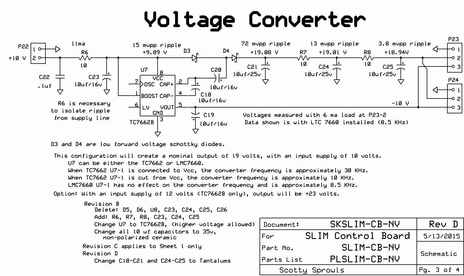
Engineering Change Notice 5-13-15.  Capacitors that had been called out as 10 ufd ceramics should be replaced with Tantalums. They are: C5, C8, C9, C18-C21, and C23-C25. See Parts Lists.
Updated 5-13-15.  Change page to reflect ECN, Control Board is Revision D.  The schematic is rev D, the parts list is rev D, the PWB remains rev C. The Parts List, PLSLIM-CB-NV has been split into four sections and moved to this web page.

SLIM-CB-NV,  Control Board, size-C
Use your mouse's "right click" and "Save Link" to download the current versions:
a. 
SKSLIM-CB-NV.sch rev D, Schematic of SLIM Control Board, in ExpressPCB software.
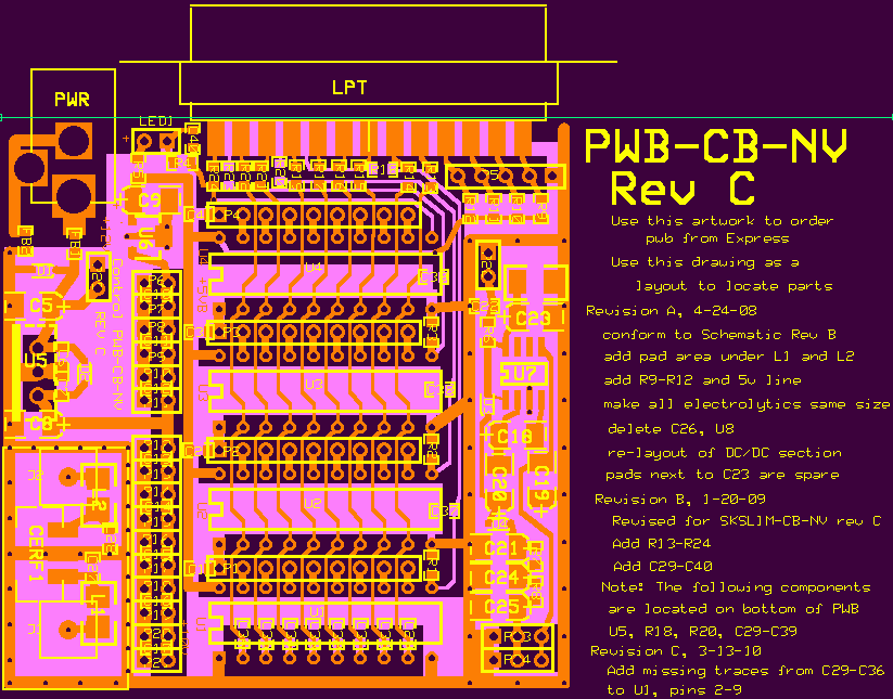
b.  PWB-CB-NV.pcb rev C, Base artwork for PWB, in ExpressPCB software.  Use this drawing to order the pwb from Express, or use as Layout to locate the parts on the SLIM Control Board.
c.  PLSLIM-CB-NV rev D, Parts Lists for SLIM Control Board are on this Web page only.

Revision D: Released 5-13-2015
Revision D is a change to capacitors in the Power Conditioner and Voltage Converter sections. In a previous revision, 10 ufd Tantalum capacitors had been changed to ceramics. Due to the ineptitude of this designer (Scotty), this was a bad decision and the ceramics must be changed back to Tantalums. The capacitors involved are: C5, C8, C9, C18-C21, and C23-C25.

    The SLIM-CB-NV Control Board is the Interface between the Computer and other SLIMs.  It consists of 4 sections; Latch, Power Conditioner, Voltage Converter, and Noise Filter. Each section is independent of the others. If a section not needed, the components need not be installed on the pwb.
    The Latch Section is a buffer between the computer and the CMOS data inputs of user modules or other devices. Eight lines of parallel data from the computer (or USB converter) are latched into one of four eight line buffers. Four output signal lines are for sending data back to the computer (or USB converter).
    The Power Conditioner accepts +12v to +15v and regulates it to +10 volts (1 amp) and to +5v (100 ma max). The section contains pin headers to distribute the +10 volts to user modules or other devices.
    The Voltage Converter Section accepts +10 volts and converts it to +20v and -10 volts.
    The Noise Filter Section is an area on the pwb to build a simple ceramic filter circuit.


Latch Section
Schematic of Latch Section, sheet 1 of 4.  Click on drawing to enlarge for viewing.
skslim_cb_nv1.gif
    The Latch Section consists of 4 ea, TTL input compatible Buffer Latches with +5 volt CMOS outputs. The design allows TTL (or 3.3 to 5 volt CMOS) inputs from the Computer's Standard LPT printer port, or a USB converter, on a DB-25 female connector (LPT). The outputs of the latches are accessible on 4 ea, 9-pin connector headers (P1-P4). All 4 of the latch I.C.'s are fed by external Parallel Data from the Computer (or USB converter).  The Data will be passed to the latch's output when it's enable line is commanded high.  If enable is kept high, the output data will follow the input data.  When the enable is brought low, the output data will be retained as a latch.  Note: Although connector headers are called out on the parts list, they are not mandatory.  Direct wiring to the other modules is optional.
    A fifth connector (P5) is a direct connection for four, open collector signals that are "read" by the Computer as "status".  Two of these are used in the MSA system, WAIT and ACK. The other two status lines, PE and SELECT are not used by the MSA or VNA, but may be in the future. Some home computers do not have internal pull-up resistors for these four lines. If so,
add 2.2 K ohm pull up resistors to these 4 status lines. Since only WAIT and ACK lines are presently used in the MSA system, only those two may need these resistors.  Here is a test to see if the pull-up resistors are required.  Re-boot the home computer.  Use a voltmeter to measure from computer ground to LPT port, pins 10, 11, 12, and 13.  If any one of these pins measures greater than +2.0 volts, the pull-ups are not required. If the Cypress USB converter is used, the pull-up resistors, R9-R12 must be removed.
    The SLIM Control Board is a generic module that is integrated into a higher assembly.  Therefore, the output signal names in the schematic are generic.  For example, a data signal that exits the computer is called D0. It is buffered by one of the four latches, U1-U4.  The name changes at the output of each latch, for example, P1D0 or P2D0, etc.
Once the Control Board is integrated into a higher assembly, the external signals are assigned more meaningful names.
    Notes, 4-12-18: The serial input resistors, R13-R24 and shunt capacitors, C29-C40 are intended to supress noise on long LPT cables from noisy computer parallel ports. If the Cypress USB board is used as the control interface, these components are not required, however, they can be left in place. Shunt resistors, R1-R4 are intended to hold the latch enable signals "low" in case the LPT connector is ever removed from the control interface during operation.

PLSLIM-CB-NV.  Parts List for Latch Section
Revision D, 5-13-2015   (updated 1-23-2016)
Designator    Value             Mfg. Part Number                     Digikey Number          Appx Cost       Notes
C1               .1 uF          C0805C104K3RACTU                       399-1168-1-ND             0.05   
C2
               .1 uF          C0805C104K3RACTU                       399-1168-1-ND             0.05   
C3               .1 uF          C0805C104K3RACTU                       399-1168-1-ND             0.05   
C4               .1 uF          C0805C104K3RACTU                       399-1168-1-ND             0.05   
C29           100 pF         C0805C101K5GACTU                       399-1121-1-ND              0.05   
C30
           100 pF         C0805C101K5GACTU                       399-1121-1-ND              0.05   
C31           100 pF         C0805C101K5GACTU                       399-1121-1-ND              0.05   
C32           100 pF         C0805C101K5GACTU                       399-1121-1-ND              0.05   
C33           100 pF         C0805C101K5GACTU                       399-1121-1-ND              0.05   
C34           100 pF         C0805C101K5GACTU                       399-1121-1-ND              0.05   
C35           100 pF         C0805C101K5GACTU                       399-1121-1-ND              0.05   
C36           100 pF         C0805C101K5GACTU                       399-1121-1-ND              0.05   
C37           100 pF         C0805C101K5GACTU                       399-1121-1-ND              0.05   
C38
           100 pF         C0805C101K5GACTU                       399-1121-1-ND              0.05   
C39           100 pF         C0805C101K5GACTU                       399-1121-1-ND              0.05   
C40           100 pF         C0805C101K5GACTU                       399-1121-1-ND              0.05   
LPT          DB-25          Norcomp 171-025-203L001                       225FE-ND              1.37    error, was 224FE-ND
P1          Conn, 9 pin     Sold as a row of 36 pins                    S1012E-36-ND                 0.27   was S1012-36-ND
P2          Conn, 9 pin     Sold as a row of 36 pins                    S1012E-36-ND                 0.27   was S1012-36-ND
P3
          Conn, 9 pin     Sold as a row of 36 pins                    S1012E-36-ND                 0.27   was S1012-36-ND
P4
          Conn, 9 pin     Sold as a row of 36 pins                    S1012E-36-ND                 0.27   was S1012-36-ND
P5          Conn, 5 pin     
Sold as a row of 36 pins                    S1012E-36-ND                 0.15   was S1012-36-ND
R1              10K            MCR10EZHF10.0K                        RHM10.0KCCT-ND          0.04
R2
              10K            MCR10EZHF10.0K                        RHM10.0KCCT-ND          0.04
R3              10K            MCR10EZHF10.0K                        RHM10.0KCCT-ND          0.04
R4              10K            MCR10EZHF10.0K                        RHM10.0KCCT-ND          0.04
R9             2.2K            MCR10ERTF2201                          RHM2.20KCHCT-ND       0.04  was MCR10EZHF2201/ RHM2.20KCCT-ND
R10           2.2K            MCR10ERTF2201                          RHM2.20KCHCT-ND       0.04  was MCR10EZHF2201/ RHM2.20KCCT-ND
R11           2.2K            MCR10ERTF2201                          RHM2.20KCHCT-ND       0.04  was MCR10EZHF2201/ RHM2.20KCCT-ND
R12           2.2K            MCR10ERTF2201                          RHM2.20KCHCT-ND       0.04  was MCR10EZHF2201/ RHM2.20KCCT-ND
R13              1K            MCR10EZHF1001                          RHM1.00KCCT-ND          0.04
R14
             1K            MCR10EZHF1001                          RHM1.00KCCT-ND          0.04
R15              1K            MCR10EZHF1001                          RHM1.00KCCT-ND          0.04
R16              1K            MCR10EZHF1001                          RHM1.00KCCT-ND          0.04
R17              1K            MCR10EZHF1001                          RHM1.00KCCT-ND          0.04
R18              1K            MCR10EZHF1001                          RHM1.00KCCT-ND          0.04
R19              1K            MCR10EZHF1001                          RHM1.00KCCT-ND          0.04
R20              1K            MCR10EZHF1001                          RHM1.00KCCT-ND          0.04
R21              1K            MCR10EZHF1001                          RHM1.00KCCT-ND          0.04
R22              1K            MCR10EZHF1001                          RHM1.00KCCT-ND          0.04
R23              1K            MCR10EZHF1001                          RHM1.00KCCT-ND          0.04
R24              1K            MCR10EZHF1001                          RHM1.00KCCT-ND          0.04
U1       Buffer/Latch         74ACT573N                                  296-4438-5-ND                0.64 was 74ACT573PC/74ACT573PC-ND
U2       Buffer/Latch         74ACT573N                                  296-4438-5-ND                0.64 was 74ACT573PC/74ACT573PC-ND
U3       Buffer/Latch         74ACT573N                                  296-4438-5-ND                0.64 was 74ACT573PC/74ACT573PC-ND
U4       Buffer/Latch         74ACT573N                                  296-4438-5-ND                0.64 was 74ACT573PC/74ACT573PC-ND
PWB    Circuit Board      PWB-CB-NV                                                                       13.11

Power Conditioner Section

Schematic of Power Conditioner Section, sheet 2 of 4
slim/skslim_cb_nv2.gif
    The Power Conditioner receives a nominal +12 volts to +13.6 volts and outputs +10 volts to multiple, 2-pin power connectors that connect to the other SLIMs. Connectors are not required and point to point soldered wires is just fine.
    U6 regulates to +5v and is intended to be used only for the Control Board latches and LED. It can supply only about 50 ma. The maximum total output current allowed through U5 is 1 amp.
 D1 is used as a reverse protection diode.  If the power input is shorted during operation, D2 should protect U5 from a reverse current destruction. Both D1 and D2 can be substituted with any silicone diode.
    FB1 and FB2 do very little for EMI.  They are there to act as fuses in case of reversed polarity input.
    U5 is to be mounted on the PWB from the bottom side of the pwb, with it's heat sink tab facing away from the pwb.
U5 will dissipate approximately 3 watts and must be "heat sinked". It is intended to be bolted to the  metal case that is housing the Control Board. The Verification MSA housing is made from .062 double side copper clad and heat dispersion is quite adequate without any additional heat sinking.
    The input voltage range is expected to be in the range of +12v to +13.6v.  However, up to +16 volts is allowed.
    P25 is intended to supply raw voltage to the Voltage Converter section as an option. If not used this way, P25 can be used to supply a cooling fan. If a fan is used, its input voltage lines must have good line filtering to prevent "hash" from being reversely impressed on the input voltage line. Muffin fans create extreme electrical noise on its power lines.
    LED1 is mounted without cutting its leads so that it can be bent to protrude through a hole in the front panel.
    Revision D changes the capacitors
C5, C8, and C9 from ceramics back to Tantalums.

PLSLIM-CB-NV.   Parts List for Power Conditioner Section
Revision D, 5-13-2015  
(updated 1-23-2016)
Designator    Value             Mfg. Part Number                     Digikey Number          Appx Cost       Notes
C5             10uf/25v        AVX, F951E106KBAAQ2                 478-8495-1-ND             1.11             Rev D
C6             .1 uF             C0805C104K3RACTU                      399-1168-1-ND             0.05   
C7
             .1 uF             C0805C104K3RACTU                      399-1168-1-ND             0.05   
C8             10uf/16v       AVX, TPSB106K016R0500               478-5230-1-ND             0.65             Rev D
C9
             10uf/16v       AVX, TPSB106K016R0500               478-5230-1-ND             0.65             Rev D
C10             .1 uF             C0805C104K3RACTU                    399-1168-1-ND             0.05   
C11             .1 uF             C0805C104K3RACTU                    399-1168-1-ND             0.05   
C12             .1 uF             C0805C104K3RACTU                    399-1168-1-ND             0.05   
C13             .1 uF             C0805C104K3RACTU                    399-1168-1-ND             0.05   
C14             .1 uF             C0805C104K3RACTU                    399-1168-1-ND             0.05   
C15             .1 uF             C0805C104K3RACTU                    399-1168-1-ND             0.05   
C16             .1 uF             C0805C104K3RACTU                    399-1168-1-ND             0.05   
C17             .1 uF             C0805C104K3RACTU                    399-1168-1-ND             0.05   
D1          Diode, Shky       ZLLS400TA                                  ZLLS400TACT-ND         0.46           Rev D
D2
          Diode, Shky       ZLLS400TA                                  ZLLS400TACT-ND         0.46           Rev D
FB1        Ferite Bead         BLM21PG221SN1D                       490-1054-1-ND              0.06   
FB2
        Ferite Bead         BLM21PG221SN1D                       490-1054-1-ND              0.06   
LED1      LED 5MM         SSL-LX5093GD                               67-1098-ND                 0.11   
P6
       Conn, 2 pin         Sold as a row of 36 pins                      S1012E-36-ND              0.06 was S1012-36-ND
P7
       Conn, 2 pin         Sold as a row of 36 pins                      S1012E-36-ND              0.06 was S1012-36-ND
P8       Conn, 2 pin         Sold as a row of 36 pins                      S1012E-36-ND              0.06 was S1012-36-ND
P9       Conn, 2 pin         Sold as a row of 36 pins                      S1012E-36-ND              0.06 was S1012-36-ND
P10     Conn, 2 pin         Sold as a row of 36 pins                      S1012E-36-ND              0.06 was S1012-36-ND
P11     Conn, 2 pin         Sold as a row of 36 pins                      S1012E-36-ND              0.06 was S1012-36-ND
P12     Conn, 2 pin         Sold as a row of 36 pins                      S1012E-36-ND              0.06 was S1012-36-ND
P13     Conn, 2 pin         Sold as a row of 36 pins                      S1012E-36-ND              0.06 was S1012-36-ND
P14     Conn, 2 pin         Sold as a row of 36 pins                      S1012E-36-ND              0.06 was S1012-36-ND
P15     Conn, 2 pin         Sold as a row of 36 pins                      S1012E-36-ND              0.06 was S1012-36-ND
P16     Conn, 2 pin         Sold as a row of 36 pins                      S1012E-36-ND              0.06 was S1012-36-ND
P17     Conn, 2 pin         Sold as a row of 36 pins                      S1012E-36-ND              0.06 was S1012-36-ND
P18     Conn, 2 pin         Sold as a row of 36 pins                      S1012E-36-ND              0.06 was S1012-36-ND
P19     Conn, 2 pin         Sold as a row of 36 pins                      S1012E-36-ND              0.06 was S1012-36-ND
P20     Conn, 2 pin         Sold as a row of 36 pins                      S1012E-36-ND              0.06 was S1012-36-ND
P21     Conn, 2 pin         Sold as a row of 36 pins                      S1012E-36-ND              0.06 was S1012-36-ND
P25     Conn, 2 pin         Sold as a row of 36 pins                      S1012E-36-ND              0.06 was S1012-36-ND
U5         LM7810           UA7810CKCS   10v Reg.                   296-21621-5-ND            0.89    was UA7810CKC/296-1975-5-ND
U6           78L05            78L05ACU        5v Reg.                         497-1183-1-ND          0.77         
PWR    Pwr Conn           CP-002A                                               CP-002A-ND            0.38   
R5         150 ohm           MCR10ERTF1500                            RHM150CHCT-ND        0.04  was
MCR10EZHF150/RHM150CCT-ND

Voltage Converter Section

Schematic of Voltage Converter,  sheet 3 of 4
slim/skslim_cb_nv3.gif
    The Voltage Converter section contains a voltage doubler/voltage inverter. The MSA requires +20v output at 7 ma but no negative voltage. The section is completely surrounded by a ground trace. A fence and lid could be installed to prevent the section from transmitting noise. However, extensive testing did not indicate that this section radiated any noise. DC connections are provided on the bottom of the board, using 3-pin connectors.  If this section is not needed or if any of the outputs is not needed, the components do not need to be installed.  Because the  MSA does not require -10 volts, C18 and C19 could be deleted.
    There are 5 options for the Voltage Converter section.
1. Option 1, using the LMC7660, with 10 v input.  Nominal output voltage of +19 volts.
    The converter receives +10 volts from the Power Conditioner and converts it to +19 volts and -10 volts.
  It can supply up to 20 ma for each.  The MSA/TG requires a total of 7 ma at +19 volts.  -10 volts is not used, and components C18 and C19 may be omitted.  The output will contain a small ripple voltage with a frequency at which the LMC7660 is operating, approximately 8.5 KHz.
2. Option 2, using the TC7662, with 10 v input.  Nominal output voltage of +19 volts.  With U7 pin 1 connected to Vcc, the ripple frequency is approximately 30 kHz.  This has not been tested but should result in much lower ripple.  At this frequency it is possible that this section could begin to radiate and require fencing.
3.
Option 3, using the TC7662, with 10 v input.  Nominal output voltage of +19 volts.  With U7 pin 1 disconnected from Vcc (trace cut), the ripple frequency is approximately 10 kHz.  This has not been tested, but should give the same results as Option 1.
4.
Option 4, using the TC7662, with 12 v input.  Nominal output voltage of +23 volts.  With U7 pin 1 connected to Vcc, the ripple frequency is approximately 30 kHz.  This has not been tested but should result in low ripple.  At this frequency it is possible that this section could begin to radiate and require fencing.
5.
Option 5, using the TC7662, with 13.6 v input.  Nominal output voltage of +26 volts.  With U7 pin 1 disconnected from Vcc (trace cut), the ripple frequency is approximately 10 kHz.  This has not been tested.
    I have tested the MSA system using Option 1, only. Options 2 - 4 can be experimented with. With an output voltage of at least 18.5 volts, the MSA will have a Band 1 frequency limit of 1050 MHz.
With an output voltage of at least 21 volts, the MSA will have a Band 1 frequency limit of 1200 MHz.
    Revision D changes the capacitors C18-C21, and C23-C25 from ceramics back to Tantalums.
Modification of SLIM-CB-NV-Rev A:
    The previous SLIM Control Board, SLIM-CB-NV-Rev A, using the pwb, PWB-CB-NV Rev 0, must be modified. Using the above schematic as a guide, the following components must be incorporated.  R6, C23, R7, C24, R8, C25. The second voltage converter can be removed to allow space for these added components. Or, this modification can be added externally to the Voltage Converter Section.  This is a necessary modification to decrease noise on both the 10 volt input line and the 20 volt output line.

PLSLIM-CB-NV.  Parts List for Voltage Converter Section
Revision D, 5-13-2015  
(updated 1-23-2016)
Designator    Value             Mfg. Part Number                      Digikey Number          Appx Cost       Notes
C18          10uf/16v    AVX, TPSB106K016R0500                    478-5230-1-ND               0.65           Rev D
C19
          10uf/16v    AVX, TPSB106K016R0500                    478-5230-1-ND               0.65           Rev D
C20          10uf/16v    AVX, TPSB106K016R0500                    478-5230-1-ND               0.65           Rev D
C21          10uf/25v    AVX, F951E106KBAAQ2                       478-8495-1-ND               1.11           Rev D
C22          .1 uF          C0805C104K3RACTU                           399-1168-1-ND               0.05   
C23
          10uf/16v    AVX, TPSB106K016R0500                    478-5230-1-ND               0.65           Rev D
C24          10uf/25v    AVX, F951E106KBAAQ2                       478-8495-1-ND               1.11           Rev D
C25          10uf/25v    AVX, F951E106KBAAQ2                       478-8495-1-ND               1.11           Rev D
D3        Diode, Shky         ZLLS400TA                                 ZLLS400TACT-ND            0.46           Rev D
D4
        Diode, Shky         ZLLS400TA                                 ZLLS400TACT-ND            0.46           Rev D
P22       Conn, 2 pin     Sold as a row of 36 pins                       
S1012E-36-ND                  0.06   was S1012-36-ND
P23       Conn, 2 pin     Sold as a row of 36 pins                       S1012E-36-ND                  0.06   was S1012-36-ND
P24       Conn, 2 pin     Sold as a row of 36 pins                       S1012E-36-ND                  0.06   was S1012-36-ND
R6          10 ohm         MCR10ERTF10R0                               RHM10.0CHCT-ND         0.10  was MCR10EZHF10.0/RHM10.0CCT-ND 
R7
          10 ohm         MCR10ERTF10R0                               RHM10.0CHCT-ND         0.10  was MCR10EZHF10.0/RHM10.0CCT-ND 
R8          10 ohm         MCR10ERTF10R0                               RHM10.0CHCT-ND         0.10  was MCR10EZHF10.0/RHM10.0CCT-ND 
U7         TC7662         TC7662BEOA, Microchip              TC7662BEOA713CT-ND         1.71       

Noise Filter Section

Schematic of Noise Filter, sheet 4 of 4
slim/skslim_cb_nv4.gif
    The Noise Filter, (N) contains a Murata Ceramic Filter, having a center frequency of 10.7 MHz and a bandwidth of 150 KHz.  Included, are impedance converter networks for 50 ohm to 330 ohm.  Loss is approximately -4.5 dB.  This section is completely surrounded by a fence and lid to isolate the section from external noise.  RF connections are provided on the bottom of the board.  If this filter is not wanted, the section does not need to be populated with components.  If so, the shield is not required.
    This section could be removed from the Control Board by cutting it away with a fine tooth saw.  If left in position, only the two outside fence shields are soldered on both sides of the board.  The two "inside" fences are soldered on the top side, only.
    This section is not used for the Original or SLIM MSA, and does not need to be populated with components.

PLSLIM-CB-NV.   Parts List for Noise Filter Section
Revision D, 5-13-2015   (no changes in this section since Rev. 0)
Designator    Value                Part Number                             Digikey Number       Appx Cost      Notes
C27             100 pF              C0805C101K5GACTU                    399-1121-1-ND        0.05
C28             100 pF              C0805C101K5GACTU                    399-1121-1-ND        0.05
CERF1        10.7/.15            Murata, SFELA10M7JAA0-B0         490-1232-ND            0.59
J1                SMA OPT        Molex, 538-73391-0070                   WM5544-ND            4.74
J2                SMA OPT        Molex, 538-73391-0070                   WM5544-ND            4.74
L1               1.8 uH              MLF2012A1R8K                            445-1050-1-ND         0.41
L2               1.8 uH              MLF2012A1R8K                            445-1050-1-ND         0.41


PWB-CB-NV Rev C, Artwork and Component Locations for SLIM Control Board
slim/pwb_cb_nv.gif
    The Control board is intended to be mounted in a corner position so that the LPT connector extends to the outside of the enclosure and U5 is bolted to the side of the enclosure. Holes are drilled in the enclosure to accommodate the DB-25 size "D" connector and the two connector mounting screws. Another .25 inch hold is drilled to accommodate the LED power indicator.  This Rev C is a fix to Rev B where the added capacitors, C29-C36, did not get their pads connected to U1, pins 2-9.