SLIM-ADC-16
Analog to Digital Converter

Updated 4-30-08.
 
Update page for name changes.  No pwb or schematic changes.
Updated 7-14-08.  Parts list revised for incorrect switch (SW1, SW2) part number.
Updated 8-11-09.  Add explanation for Optional Power Modification when used with MSA/VNA
Updated 5-17-15.  Parts list revised to Rev B and moved to this page. Change capacitors for new builds. Working units need not be changed.
Updated 6-09-16.  Add LTC1864 to parts list as alternate.

SLIM-ADC-16, AtoD Converter, 16 bit, size A
Use your mouse's "right click" and "Save Link" to download the current versions:
a.
  SKSLIM-ADC-16.sch Rev 0, Schematic, in ExpressPCB software.
b.  PWB-ADC10.pcb Rev 0, Base artwork for PWB, in ExpressPCB software.  Use this drawing to order the pwb from Express, or use as Layout to locate the parts on the SLIM-ADC-16.
c.  PLSLIM-ADC-16 Rev B. Parts List. Maintained on this page, only.
d. 
Download the AD7685 data sheet at: http://www.analog.com/en/analog-to-digital-converters/ad-converters/ad7685/products/product.html

Release History
Part #: SLIM-ADC-16 Rev 0, Released 7-01-2007
Schematic: SKSLIM-ADC-16 Rev 0, Released 7-01-2007
Parts List: PLSLIM-ADC-16 Rev A, Revised 7-14-2008
PWB: PWB-ADC10 Rev 0, Released 7-01-2007

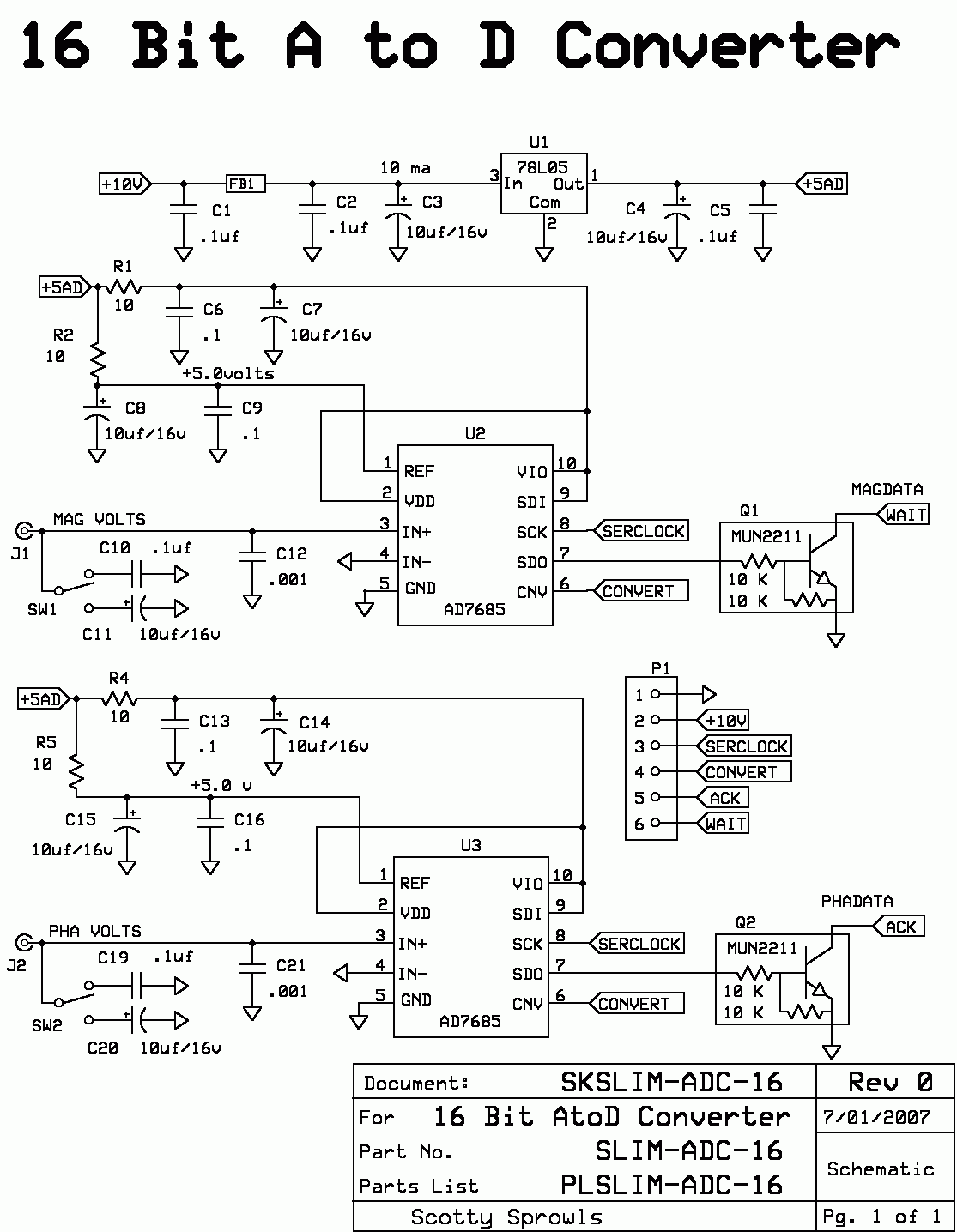
    The SLIM-ADC-16 is a dual 16 bit, serial, analog to digital converter, using two AD7685's.  There is no manual adjustment to set the A to D range.  It is not needed to obtain excellent resolution in the MSA and VNA systems.  Each AtoD will digitize its input of 0 to 5 volts to a bit value of 0 to  65535 bits.  This equates to 76.3 uv per bit.
      Both A/D's will capture, and clock out their data simultaineouslyThe software commands both U2 and U3 to begin conversion with a single toggle of the signal, "CONVERT".  16 toggles of the signal, "SERCLOCK", causes the I.C. to output a serial stream of 16 bits.  The serial SDO outputs of the AtoD I.C.'s have limited (500 ua) current capability.  Therefore, the open collectors of Q1 and Q2 provide buffering and current sinking to drive the "WAIT" and "ACK" lines to the LPT port of the Computer. The Computer's LPT port is nominally a TTL compatible input with a pull up resistor to +5 volts. It can also drive a pull-up on a +3.3v bus.
    5-17-15  For new builds, Q1 and Q2 are called out as 2N7002, FETs. This allows higher data transfer speeds.

    The circuit is designed with thru hole pads, to allow each input to be connected to an external switch. The switch selects the amount of capacitance to be placed in shunt with the input.  Each switch is a single pole, three throw, with a non-connecting center position. This allows a selection of 3 different integration times (Video Bandwidth).  This module is expected to be mounted very close to the front panel of the integrated system so that the user can mount the switches on the front panel and maintain very short leads from the switches to the bottom of the module.
    The base PWB has the part number, PWB-ADC10.  The "10" signifies the use of a 10 pin MSOP package.  There are other A/D I.C.s with this package.  More A/D SLIMs could be created from this pwb design.
  For the Basic MSA, only the U2 section needs to be populated.  The U3 section is used for the VNA extension of the MSA.
    
Updated 6-09-16. The LTC1864 can be substituted for U2 or U3. It is also a 16 bit converter, but is in an 8-pin package. If used, place its pin 1 on the pwb's pad 2.

Optional Power Modification to
SLIM-ADC-16 when used in the MSA with VNA extension:
  This optional modification allows the
SLIM-ADC-16 to be powered directly by the Phase Detector Module's regulated +5 volts. This causes both modules to use the same regulated +5 volts. This results in more accurate Phase Measurements with the VNA.
    The modification is quite simple: Remove and delete U1, the 78L05. Jumper a wire between the two pads that supported U1. The pads are U1 pin 3, to U1 pin 1. The power input at P1 pin 2 must be +5 volts, which is provided by the Phase Detector Module.

SKSLIM-ADC-16, Schematic of SLIM-ADC-16
slim/skslim_adc_16.gif

For new builds, replace Q1 and Q2 with 2N7002 FETs. No resistors need to be added.

PWB-ADC10, Artwork for pwb, and Layout for SLIM-ADC-16
slim/pwb_adc10.gif  slim/atod.JPG

How to Control the SLIM-ADC-16
   
Two lines control this module, the CONVERT and SERCLOCK.  Both AtoD chips are controlled simultaneously. Before conversion these lines are held low. To begin Conversion, the CONVERT is commanded high. This initiates the in-chip sample and hold circuit. While CONVERT is high, any voltage changes on the analog inputs will be disregarded. Also, the SDO output will be high impedance (WAIT and ACK will be high impedance).  It now takes approximately 2 usec for the 16 bit conversion (Sample) to take place and the 16 bit data word will be stored in its buffer (Hold). After 3 usec, the CONVERT signal is brought low. The MSB (D15) will be present on the SDO pin (its inversion is on the line back to the computer, WAIT or ACK).  Each time the SERCLOCK is brought low, the data word is shifted by one bit. The Data is valid 15 nsec after the negative edge of SERCLOCK. It takes 16 SERCLOCK's to shift out the 16 bit data word.
    If stored data is not clocked out of the buffer, the next
CONVERT signal will overwrite the buffer.
  The MSA Program causes this computer action:
Begins with CONVERT and SERCLOCK low.
CONVERT to high.  Initiates the A to D conversion process.
CONVERT to low. (High to low takes about 5 usec, allowing the minimum 2 usec. conversion time requirement)
SERCLOCK to high.  D15 MSB is valid on SDO. MAGDATA and PHADATA is read by computer
SERCLOCK to low.  Next data word bit is shifted.
SERCLOCK to high.  D14 bit is valid on SDO. MAGDATA and PHADATA is read by computer
SERCLOCK to low.  Next data word bit is shifted.
SERCLOCK to high.  D13 bit is valid on SDO. MAGDATA and PHADATA is read by computer
SERCLOCK to low.  Next data word bit is shifted.
SERCLOCK to high.  D12 bit is valid on SDO. MAGDATA and PHADATA is read by computer
SERCLOCK to low.  Next data word bit is shifted.
SERCLOCK to high.  D11 bit is valid on SDO. MAGDATA and PHADATA is read by computer
SERCLOCK to low.  Next data word bit is shifted.
SERCLOCK to high.  D10 bit is valid on SDO. MAGDATA and PHADATA is read by computer
SERCLOCK to low.  Next data word bit is shifted.
SERCLOCK to high.  D9 bit is valid on SDO. MAGDATA and PHADATA is read by computer
SERCLOCK to low.  Next data word bit is shifted.
SERCLOCK to high.  D8 bit is valid on SDO. MAGDATA and PHADATA is read by computer
SERCLOCK to low.  Next data word bit is shifted.
SERCLOCK to high.  D7 bit is valid on SDO. MAGDATA and PHADATA is read by computer
SERCLOCK to low.  Next data word bit is shifted.
SERCLOCK to high.  D6 bit is valid on SDO. MAGDATA and PHADATA is read by computer
SERCLOCK to low.  Next data word bit is shifted.
SERCLOCK to high.  D5 bit is valid on SDO. MAGDATA and PHADATA is read by computer
SERCLOCK to low.  Next data word bit is shifted.
SERCLOCK to high.  D4 bit is valid on SDO. MAGDATA and PHADATA is read by computer
SERCLOCK to low.  Next data word bit is shifted.
SERCLOCK to high.  D3 bit is valid on SDO. MAGDATA and PHADATA is read by computer
SERCLOCK to low.  Next data word bit is shifted.
SERCLOCK to high.  D2 bit is valid on SDO. MAGDATA and PHADATA is read by computer
SERCLOCK to low.  Next data word bit is shifted.
SERCLOCK to high.  D1 bit is valid on SDO. MAGDATA and PHADATA is read by computer
SERCLOCK to low.  Next data word bit is shifted.
SERCLOCK to high.  D0 bit is valid on SDO. MAGDATA and PHADATA is read by computer
SERCLOCK to low.  SDO is high impedance.. MAGDATA and PHADATA are "don't care"
Subsequent SERCLOCK's do nothing.

Parts List, PLSLIM-ADC-16
Revision B,  5-16-2015 (updated 1-23-2016)
Des.     Value            Part Number.                                Digikey Number      Cost             Notes
C1        .1 uF            C0805C104K3RACTU                    399-1168-1-ND        0.05   
C2        .1 uF            C0805C104K3RACTU                    399-1168-1-ND        0.05   
C3        10uf/16v    AVX, TPSB106K016R0500                478-5230-1-ND        0.65             Rev B
C4
        10uf/16v    AVX, TPSB106K016R0500                478-5230-1-ND        0.65             Rev B
C5        .1 uF            C0805C104K3RACTU                     399-1168-1-ND        0.05   
C6        .1 uF            C0805C104K3RACTU                     399-1168-1-ND        0.05   
C7
        10uf/16v    AVX, TPSB106K016R0500                 478-5230-1-ND        0.65            Rev B
C8        10uf/16v    AVX, TPSB106K016R0500                 478-5230-1-ND        0.65            Rev B
C9        .1 uF            C0805C104K3RACTU                    399-1168-1-ND        0.05   
C10      .1 uF            C0805C104K3RACTU                    399-1168-1-ND        0.05   
C11
        10uf/16v    AVX, TPSB106K016R0500             478-5230-1-ND        0.65                Rev B
C12        .001 uF        C0805C102J5GACTU                     399-1136-1-ND        0.08    was ECJ-2VC1H102J/PCC102CGCT-ND
C13        .1 uF            C0805C104K3RACTU                399-1168-1-ND            0.05
C14
        10uf/16v    AVX, TPSB106K016R0500             478-5230-1-ND          0.65              Rev B
C15        10uf/16v    AVX, TPSB106K016R0500             478-5230-1-ND          0.65              Rev B
C16        .1 uF            C0805C104K3RACTU                399-1168-1-ND            0.05
C19        .1 uF            C0805C104K3RACTU                399-1168-1-ND            0.05
C20
        10uf/16v    AVX, TPSB106K016R0500             478-5230-1-ND          0.65              Rev B
C21        .001 uF        C0805C102J5GACTU                     399-1136-1-ND        0.08    was ECJ-2VC1H102J/PCC102CGCT-ND
FB1    Ferite Bead        BLM21PG221SN1D                490-1054-1-ND                0.06   
J1       SMA Optional      Molex, 538-73391-0070            WM5544-ND                4.74   
J2
      SMA Optional      Molex, 538-73391-0070            WM5544-ND                4.74   
P1        Conn, 6 pin    sold as row of 36 pins                 S1012E-36-ND               0.18    was S1012-36-ND
Q1        MUN2211    For new builds, use 2N7002
Q2        MUN2211
    For new builds, use 2N7002
Q1-alt    2N7002        FET,  2N7002-7-F                   2N7002-FDICT-ND            0.15            Rev B.  Note 1
Q2-alt    2N7002        FET,  2N7002-7-F                   2N7002-FDICT-ND            0.15            Rev B.  Note 1
R1        10                MCR10ERTF10R0                    RHM10.0CHCT-ND          0.04    was MCR10EZHF10.0/RHM10.0CCT-ND 
R2        10               
MCR10ERTF10R0                    RHM10.0CHCT-ND          0.04    was MCR10EZHF10.0/RHM10.0CCT-ND 
R4        10                MCR10ERTF10R0                    RHM10.0CHCT-ND          0.04    was MCR10EZHF10.0/RHM10.0CCT-ND 
R5        10                MCR10ERTF10R0                    RHM10.0CHCT-ND          0.04    was MCR10EZHF10.0/RHM10.0CCT-ND 
SW1         SP2T, On-Off-On,    100SP3T1B1M1REH    EG2376-ND                    3.45            RevA, has eyelets
SW2         SP2T, On-Off-On,    100SP3T1B1M1REH    EG2376-ND                    3.45
            RevA, has eyelets
SW1-alt    SP2T, On-Off-On,    100SP3T1B1M2QEH    EG2377-ND                    3.84            RevA, has posts
SW2-alt    SP2T, On-Off-On,    100SP3T1B1M2QEH    EG2377-ND                    3.84
            RevA, has posts
U1        78L05            78L05ACU                                497-1183-1-ND                0.77    see optional Power Mod.
U2        AD7685        AD7685BRM                            AD7685BRM-ND             16.16   
U3        AD7685        AD7685BRM                            AD7685BRM-ND             16.16
U2-alt   LTC1864       LTC1864IMS8#PBF           LTC1864IMS8#PBF-ND        13.57   8-pin package
U3-alt   LTC1864       LTC1864IMS8#PBF           LTC1864IMS8#PBF-ND        13.57   8-pin package
PWB    Circuit Board    PWB-ADC10                                                                  3.28   

Note 1: The FET, 2N7002 has a much faster turn-off speed than the MUN2211 (low to open level at collector). The FET, as called out in the parts list, has the same package footprint and can be placed on the pwb pads without any modification. I suggest the 2N7002 for all new builds. Old builds do not need to change unless Q1 and Q2 are driving the Cypress converter or Beagle Bone, and have an issue with data transfer speed.