SLIM-PDM rev C
Phase Detector Module

Updated 10-21-08:  Update to reflect SLIM-PDM Revision B
Updated 2-9-09:  Update to add Schematic Error Note
Updated 8-11-09:  Update to explain voltage source option. Add revision history.
Updated 11-20-10:  Update to reflect SLIM-PDM Revision C, addition of 2 capacitors.
Updated 11-25-11:  Add links to Archived documents
Updated 5-16-15:  Change capacitors. Change Parts List to Rev D and move to this page.
Updated 1-20-16:  Update to reflect new printed wiring board, PWB-PDM Rev C. (note: there was no Rev B)

SLIM-PDM, Phase Detector Module, size-A
Use your mouse's "right click" and "Save Link" to download:
a. 
SKSLIM-PDM rev C, Schematic, in ExpressPCB software.
b.  LAYSLIM-PDM rev C, Parts Layout. For parts locations.
c.   PLSLIM-PDM Rev D. Parts List. Maintained on this page, only.
d.  PWB-PDM rev C, PWB Artwork, in ExpressPCB software. Use to order from Express.
This SLIM-PDM is constructed on a common printed wiring board, the PWB-PDM (rev C).  Previously, there was a separate web page for the PWB.  I have deleted that page and combined the information on this page.  If you have constructed the SLIM-PDM rev A, using the PWB-PDM (rev 0) board, and would like to improve the PDM accuracy, see the Modification Procedure on the end of this page.

    The SLIM-PDM is a 360 degree, Phase to Voltage Converter.  It is specifically designed to operate at 10.7 MHz, but will operate in the KHz range up to 30 MHz.  The J1 and J2 inputs can be sine or square wave .  The min / max sine input is -20 dBm to +18 dBm.  The min / max square input is 10 mvpp to 5vpp.  Input impedance is nominally 50 ohms, but can be changed to any input impedance.
    The output, at J3, is a DC voltage that is proportional to the differential phase of the input signals at J1 and J2.  The 0v to +5v output should be loaded with 100 K or higher.  A realistic measurable phase range is from 20 degrees to 340 degrees with error less than .1 degrees.
    Power requirements for the
SLIM-PDM is +7 volts to +15 volts at 50 ma.

Option when using PDM in MSA/VNA
    The PDM has a provision to source +5 volts to a separate Analog to Digital Converter module, the SLIM-ADC.  This allows both modules to use the same regulated +5volts.  This allows for more accurate Phase measurements.  The
SLIM-PDM Rev 0 requires no change or modification for this application.  Later revisions require the placement of FBx.

Engineering Change Notice, ECN-11-20-2010
    Although rare, the PDM rev B may have a tendency to "self oscillate". A modification is made to prevent this rare instability.
If your PDM rev B is operating normally you may omit the modification. To modify and update SLIM-PDM-revB into SLIM-PDM-revC, the addition of two capacitors is necessary (C24 and C25). See schematic, SKSLIM-PDM Rev C. Also see LAYSLIM-PDM-Rev C.
When building a new SLIM-PDM rev C using the PWB-PDM Rev A, the capacitors do not have pwb pads and should be placed according to the layout (see below). Adding the jumper wire to U9-6 (or U9-3) is difficult since the IC is so small. I would suggest the PDM be built and tested in its final configuration before this modification is performed. It may not even be necessary.
    This ECN is incorporated on the
PWB-PDM Rev C. (see below)

Layout and parts locator for SLIM-PDM
slim/layslim_pdm.gif  slim/pwb_pdm.gif
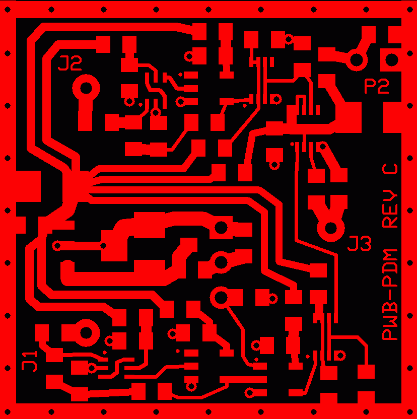
Updated 1-20-16:     The document "layslim_pdm.gif" is used to locate parts on the board.  To order PWB from Express, use pwb-pdm.pcb
    Note: The layout and schematic show that there are two ferrite beads supplying U5, FBx and FB2.  The installation of these beads is determined by how the SLIM-PDM is used in a final configuration of a high level system.


SKSLIM-PDM, Schematic of SLIM-PDM
slim/skslim_pdm.gif
    Powering Options: 
    If the PDM is used as an independent module (not in a system), install FBx and delete FB2.
    If the PDM is used to source its regulated +5 volts to another module via P2, install both FBx and FB2. This is the configuration for the MSA/VNA. The PDM supplies the Analog to Digital Converter with +5 volts.
    If an external +5 volts is used to supply the entire PDM via P2,
install both FBx and FB2, and delete U1 (this option is not recommended).
    If an external +5 volts is used to supply only the final stage of the PDM, delete FBx and install FB2
(this option is no longer recommended).

Parts List, PLSLIM-PDM
Revision D,    5-16-2015 (updated 1-24-2016)
Des.        Value       Part Number                           Digikey Number       Cost            Notes

C1        .01 uF        C0805C103K5RACTU                399-1158-1-ND       0.04   
C2        .1 uF         C0805C104K3RACTU                399-1168-1-ND         0.05   
C3        10uf/16v    
AVX, TPSB106K016R0500         478-5230-1-ND        0.65            Rev D
C4        .1 uF         C0805C104K3RACTU                399-1168-1-ND         0.05   
C5       10uf/16v    
 AVX, TPSB106K016R0500         478-5230-1-ND        0.65            Rev D
C6        100 pF        C0805C101K5GACTU            399-1121-1-ND            0.05   
C7        .1 uF          C0805C104K3RACTU            399-1168-1-ND            0.05   
C8        .1 uF          C0805C104K3RACTU                399-1168-1-ND         0.05   
C9        .1 uF          C0805C104K3RACTU                399-1168-1-ND        0.05   
C10    .1 uF            C0805C104K3RACTU            399-1168-1-ND            0.05   
C11    .1 uF            C0805C104K3RACTU            399-1168-1-ND            0.05   
C12    .1 uF            C0805C104K3RACTU            399-1168-1-ND            0.05   
C13    .1 uF            C0805C104K3RACTU            399-1168-1-ND            0.05   
C14    .01 uF          C0805C103K5RACTU                399-1158-1-ND         0.04   
C15    .01 uF          C0805C103K5RACTU                399-1158-1-ND         0.04   
C16    .01 uF          C0805C103K5RACTU                399-1158-1-ND         0.04   
C17                        Rev A, deleted
C18                        Rev A, deleted
C19    .01 uF          C0805C103K5RACTU                399-1158-1-ND         0.04   
C20    .1 uF           C0805C104K3RACTU                399-1168-1-ND         0.05            Rev B, added
C21    .1 uF           C0805C104K3RACTU                399-1168-1-ND         0.05            Rev B, added
C22    .1 uF           C0805C104K3RACTU                399-1168-1-ND         0.05            Rev B, added
C23    10uf/16v    
 AVX, TPSB106K016R0500         478-5230-1-ND          0.65            Rev D
C24    22 pfd        C0805C220J5GACTU                  399-1113-1-ND          0.10            Rev C, added
C25    22 pfd        C0805C220J5GACTU                  399-1113-1-ND          0.10            Rev C, added
                         22 pfd was size 0603, in error. Changed 1-24-16
FB1                        Rev A, deleted
FB2    Ferite Bead    BLM21PG221SN1D                490-1054-1-ND          0.06   
J1-opt    SMA OPT    Molex, 538-73391-0070            WM5544-ND           4.74       
J2-opt    SMA OPT    Molex, 538-73391-0070            WM5544-ND           4.74       
J3-opt    SMA OPT    Molex, 538-73391-0070            WM5544-ND           4.74       
L1                        Rev A, deleted
L2                        Rev A, deleted
P1    Conn, 3 pin     Sold as row of 36 pins              S1012E-36-ND             0.09    was
S1012-36-ND
P2    Conn, 2 pin     Sold as row of 36 pins              S1012E-36-ND             0.06    was S1012-36-ND
R1    49.9            MCR10ERTF49R9                RHM49.9CHCT-ND          0.04    was MCR10EZHF49.9/RHM49.9CCT-ND
R2    100K          MCR10ERTF1003                 RHM100KCHCT-ND        0.04    was MCR10EZHF100K/RHM100KCCT-ND
R3    0                MCR10EZHJ0.0                        RHM0.0ACT-ND           0.08        Rev A, change from 10 ohms
R4    10              MCR10ERTF10R0                    RHM10.0CHCT-ND       0.04    was
MCR10EZHF10.0/RHM10.0CCT-ND
R5    10K            MCR10EZHF10.0K                  RHM10.0KCCT-ND       0.04   
R6    0                MCR10EZHJ0.0                    RHM0.0ACT-ND               0.08        Rev A, change from 10 ohms
R7    49.9           
MCR10ERTF49R9                RHM49.9CHCT-ND          0.04    was MCR10EZHF49.9/RHM49.9CCT-ND
R8    10              MCR10ERTF10R0                    RHM10.0CHCT-ND       0.04    was MCR10EZHF10.0/RHM10.0CCT-ND
R9    100K          MCR10ERTF1003                 RHM100KCHCT-ND        0.04    was MCR10EZHF100K/RHM100KCCT-ND
R10                        Rev A, deleted
R11    10            
MCR10ERTF10R0                    RHM10.0CHCT-ND       0.04    was MCR10EZHF10.0/RHM10.0CCT-ND
R12                         Rev B, deleted
R13    10            
MCR10ERTF10R0                    RHM10.0CHCT-ND       0.04    was MCR10EZHF10.0/RHM10.0CCT-ND
R14    10            MCR10ERTF10R0                    RHM10.0CHCT-ND       0.04    was MCR10EZHF10.0/RHM10.0CCT-ND
R15    10            MCR10ERTF10R0                    RHM10.0CHCT-ND       0.04    was MCR10EZHF10.0/RHM10.0CCT-ND
U1    78L05        78L05ACU                                    497-1183-1-ND         0.77   
U2    7WZU04    NC7WZU04P6X                NC7WZU04P6XCT-ND       0.37    Do not substitute
U3    7SZ04        NC7SZ04M5X                   NC7SZ04M5XCT-ND         0.33   
U4    74LVC1G86    SN74LVC1G86DBVR            296-9853-1-ND           0.36   
U5    7SZ74        NC7SZ74K8X                    NC7SZ74K8XCT-ND         0.4   
U6    7WZU04    NC7WZU04P6X                NC7WZU04P6XCT-ND       0.37    Do not substitute
U7    7SZ04        NC7SZ04M5X                    NC7SZ04M5XCT-ND         0.33   
U8    7SZ74        NC7SZ74K8X                    NC7SZ74K8XCT-ND          0.40   
U9    7SZ74        NC7SZ74K8X                    NC7SZ74K8XCT-ND          0.40        Rev B, added
PWB    Circuit Board    PWB-PDM-RevC                                                3.28

Description of the Phase Detector Circuit
    The J1 (Reference) signal is buffered and squared by U2 and U3, and then applied to the input of U4.  U4 can be externally commanded to output the signal normally, or inverted (180 degree phase change).  U4's output signal (positive going, leading edge) triggers U9 to change it's output state to "1".  It will immediately reset to "0", creating about a 10 nsec, "one shot" (Note: see the Engineering Change Notice earlier on this page).   U9's output (positive going, leading edge), triggers U5 to change it's output state to "0".  U5's output will remain in a stable state of "0" until it receives a "clear" signal on it's pin 6.
    The J2 (Input) signal is buffered and squared by U6 and U7.  U7's output signal (positive going, leading edge) triggers U8 to change it's output state to "0".  It will immediately reset to "1", creating about a 10 nsec, "one shot" (Note: see the Engineering Change Notice earlier on this page).   U8's output (negative going, leading edge), clears U5 to guarantee it's output state at "1".  U5's output will remain in a stable state of "1" until it receives the next "clock" signal on it's pin 1.
    Note: U2 and U6 are low current, self biased buffer amplifiers, to allow either sine or square inputs.  Do not substitute these components without design consideration of power consumption.
    The output of U5 is a series of square waves with a duty cycle dependent on the amount of time that U5 is in a "0" state or in a "1" state.  This duty cycle represents the ratio of the phase of it's two input signals.  The U5 output is coupled to a resistor and capacitor, which filters out the high frequency square waves.  This leaves an integrated DC voltage that will vary from 0 volts to + 5 volts, depending on the phase difference of the two input signals.  This DC signal is called Phase Volts, at J3.  The integration filter is not low impedance, due to the 10 K ohm series integration resistor.  Therefore, any load connected to J3 must be high impedance to prevent excessive loading.  Loading should be 100 K ohms or greater.  The input resistance of 1 Meg ohms, typical of digital voltmeters or Analog to Digital Converters is the expected load for the PDM.

Uncertainties and Non-linearities of the SLIM-PDM (The Dead Zone)
    If this were a "perfect" Phase Detector, and the two input signals were in phase by 0 degrees, the output voltage would be 0 volts.  If the two signals were out of phase by 360 degrees, the output voltage would be +5.0 volts.  Since there is no difference between 0 degrees and 360 degrees, a Phase Detector would be "confused", and it's output would not "know" whether to output 0 volts or +5.0 volts.  This is an "indeterminate" phase detection area and the output will be very noisy.  Also, this phase detector has an area that is non-linear, due to several factors.  The time durations of the two pulses controlling U5, the internal speed of U5, and the rise/fall times of the input signals and output signal.  This area of uncertainty and non-linearity is simply called the "dead zone".  It occurs from about -20 degrees to about +20 degrees from when the two input signals are in phase (0/360).
  This is the reason for U4 to invert the Reference input signal and change it's phase by 180 degrees when the phase detector approaches, or is in the "dead zone".  This phase inversion of 180 degrees can be subtracted from the final measurement results if U4 has been commanded to "invert".  However, due to the internal speed of U4, this will not be exactly 180 degrees.  It will be quite close, but it needs to be measured and substituted for the theoretical 180 degree phase inversion.

Converting Phase to Voltage
    Assume, for the moment, that this Phase Detector is "perfect".  That is, no "dead zone".  It has a full dynamic range of 360 degrees.  If the Reference signal is the only signal entering the phase detector, the U5 output will remain in a "0" state.  When the Input signal is applied, U5 will be forced to change it's output state to "1" and it will remain there until the next reference pulse.
   
Now, let us assume the Input signal lags the Reference signal by 1 degree.  The Reference signal triggers U5 into the "0" state.  Then, after 1 degree, the Input signal forces U5 into the "1" state.  It remains in the "1" state until the next Reference pulse.  And, this will not occur until 359 degrees later.  Therefore, the output of the U5 will be a square wave with a duty cycle (low for 1/360 of the time and high for 359/360 of the time).  The integrated DC Phase Volts will be equal to (360-1)/360 x 5.0v, or 359/360 x 5v.  This would be 4.98611 volts.
     Now, assume the Input signal lags the Reference signal by 10 degrees.  The Reference signal triggers U5 into the "0" state.  Then, after 10 degrees, the Input signal forces U5 into the "1" state.  It remains in the "1" state until the next Reference pulse, which occurs 350 degrees later.  The output of the U5 now has a duty cycle, of low for 10/360 of the time and high for 350/360 of the time.  The integrated DC Phase Volts will be equal to (360-10)/360 x 5.0v.  This would be 4.8611 volts.
    For both cases, the
output voltage is proportional to the amount of time the output of U5 is high compared to the total period.  The following computations are used to determine the output voltage:
    If Input lags Reference by 1 degrees, then (360-1)/360 x 5.0v = 4.98611 volts
    If Input lags Reference by 10 degrees, then (360-10)/360 x 5.0v = 4.8611 volts
    If Input lags Reference by 45 degrees, then (360-45)/360 x 5.0v = 4.375 volts
    If Input lags Reference by 72 degrees, then (360-72)/360 x 5.0v = 4.000 volts
    If Input lags Reference by 90 degrees, then (360-90)/360 x 5.0v = 3.750 volts
    If Input lags Reference by 180 degrees, then (360-180)/360 x 5.0v = 2.500 volts
    If Input lags Reference by 270 degrees, then (360-270)/360 x 5.0v = 1.250 volts
    If Input lags Reference by 288 degrees, then (360-288)/360 x 5.0v = 1.000 volts
    If Input lags Reference by 315 degrees, then (360-315)/360 x 5.0v = 0.625 volts
    If Input lags Reference by 350 degrees, then (360-350)/360 x 5.0v = 0.1389 volts
    If Input lags Reference by 359 degrees, then (360-359)/360 x 5.0v = 0.01389 volts 
Since the SLIM-PDM is not perfect, and has a "dead zone", data taken below 45 degrees and above 315 degrees is subject to greater error than the range between 45 and  315 degrees.
    The calculations, above, assumed that the voltage applied to the phase detector (U5) is exactly +5.0 volts.  This will never be the case, and is not important.  In the formulas, substitute the 5.0v with the actual voltage applied to U5 pin 8.  In the SLIM-PDM, it will be between +4.90 and +5.10 volts, due to the tolerance of the voltage regulator (U1), or the external reference applied at P2.

Using the Phase Detector Module
    The SLIM-PDM can be used as a "stand-alone" module for phase to voltage conversion.  If so, it must be calibrated for the use it is intended.  The user should be aware that sine wave inputs must be amplitude stable for accurate results.  Otherwise, AM to PM conversion error is introduced by the buffer amplifiers (U2 and U6), although minimal.  Temperature changes will also effect the accuracy.
    When the
SLIM-PDM is integrated into a higher level system, the same conditions exist.  I designed this SLIM-PDM specifically to be integrated into a Vector Network Analyzer.  The SLIM-PDM's voltage output is coupled to a Voltage to Digital converter (SLIM-ADC). This combination is a Phase to Digital Converter, bypassing the voltage conversion algorithms.  The conditional phase errors of the PDM are calibrated at a system level, rather than at a module level.

Updated 10-21-08  Modification of the SLIM-PDM-revA (only)
    The following modifications (1-4) can be performed to increase the phase measurement accuracy of the SLIM-PDM-revA only. Later revisions are not affected.  If the builder is satisfied with phase measurements that are accurate to +/- 1 degree, the MODS 1-4 need not be done.  These mods will increase the accuracy of the PDM to about .1 degrees and the total accuracy of the VNA system to about +/- .2 degrees.

Pictures of SLIM-PDM-revA and modifications to increase performance.
  slim/pdm.JPG  slim/modpdm.jpg
    The first photo is the SLIM-PDM-revA without modifications.  It uses the Rev 0 version of the PWB.  The second photo shows where to cut the traces and add components.

MOD 1: Fix phase error caused by Fairchild '74 flip-flop.  The internal timing of U5 is affected if it's clock signal at it's pin 1 is at a high level when it is "cleared" at Pin 6.
a. Cut trace between U4-4 and U5-1, see "x" in photo (on top of capacitor)
b. Install a 10 pfd capacitor in series between U4-4 and U5-1 (the cap with "x")
c. Install a 1.0 K ohm resistor from U5-1 to ground at C9.
This modification creates a "spike" for triggering U5.  This is an easier modification than adding another "one-shot".

MOD 2: To decrease circuit cross-talk, via the common power traces. This separates the common 5v feed from U1 to individual feeds.
a. Cut the +5volt power trace between the junctions of R3, R4, R6, R8.
  The trace between R3 and R4 is kept intact and the trace between R6 and R8 is kept intact. The short trace length between these two junction paths is what is cut.  see "X" in photo
b. Add a jumper wire (22 to 26 ga.) from C5 (+5v) to the junction path connecting R6 and R8. (--5v)
This modification helps isolate the Limiter squaring circuit from the Reference squaring circuit.

MOD 3: Increase linearity of Reference buffer circuit, U2 and U3.
a.  Remove R2.  Install R2 (on it's side) on U3-4.  Add a jumper wire from the open end of R2 to the junction trace of C12 and R1 (where R2 was removed).
b. Cut +5volt power trace between the junction of R3 and C7. see "X"
c. Add a .1 ufd capacitor from R3 (U3-5) to the ground at C10.
d. Install a 10 ohm chip resistor at the +5v junction of C7. Stand it on end.  Attach a jumper wire from the open end of the 10 ohm resistor to C5 (+5v).  see "5v ------"
This modification isolates U2 from U3, which makes the buffering action of U2 more linear.

MOD 4: Allows the Phase Detector IC (U5) to be powered by the SLIM-ADC module.  This modification is for better phase accuracy in the VNA system.  It requires modifications in two modules, the SLIM-PDM and the SLIM-ADC

I.  Modification to SLIM-PDM:
a. Install FB1 and C19. Installing P2 is optional.
b. Cut 5 volt power trace between C5 and ferrite bead, FB1.  see "X"
c. Install a 10 uf capacitor between FB1 and the ground at U5-4

II.  Modification to SLIM-ADC-16 (or SLIM-ADC-12):
d. If an external wire is connected between the SLIM-PDM-P2-2 and the
  SLIM-ADC-P1-2, remove it. (corrected error on 11-22-09, was SLIM-PDM-P2-1)
e. Install U1 (remove jumper under U1 if installed)
f. Drill a hole (appx 0.020 inch dia) next to U1-1. Trim away ground
  plane on bottom side to prevent shorting.
g. Insert a wire (22 to 26 ga.) into hole from bottom.
    Bend end of wire over the +5v trace at U1-1, and solder.
    Connect other end of wire to SLIM-PDM-P2-2.
(corrected error on 11-22-09, was SLIM-PDM-P2-1)
Now, the SLIM-ADC-16 (-12) will supply +5v power to phase detector
  flip-flop (U5) in the SLIM-PDM.  (appx. 1.6 ma)