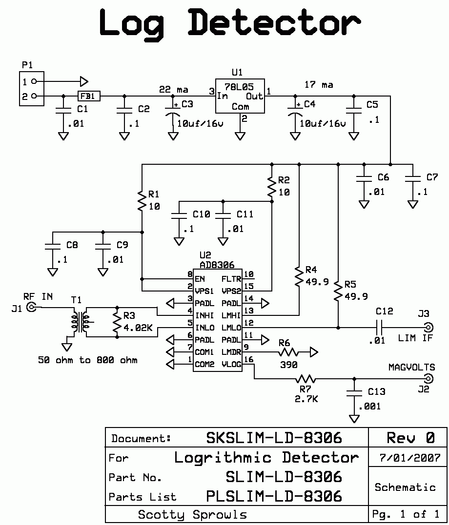
SLIM-LD-8306
Logarithmic Detector


Updated 8-05-09 Added information on experimental modification.
Updated 
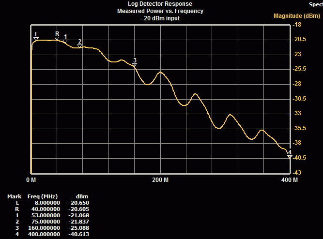
4-5-15 Add Log Det Response Plot
Updated 5-18-15  Change filter capacitors, Change Parts List to Rev A and move to this page.
Updated 12-26-15  No real changes, just some clean-up.

SLIM-LD-8306, Log Detector, size-A
Use your mouse's "right click" and "Save Link" to download the current versions:
a
.   SKSLIM-LD-8306.sch Rev 0, Schematic, in ExpressPCB software.
b.   PWB-LD-8306.pcb Rev 0, Base artwork for PWB, in ExpressPCB software.  
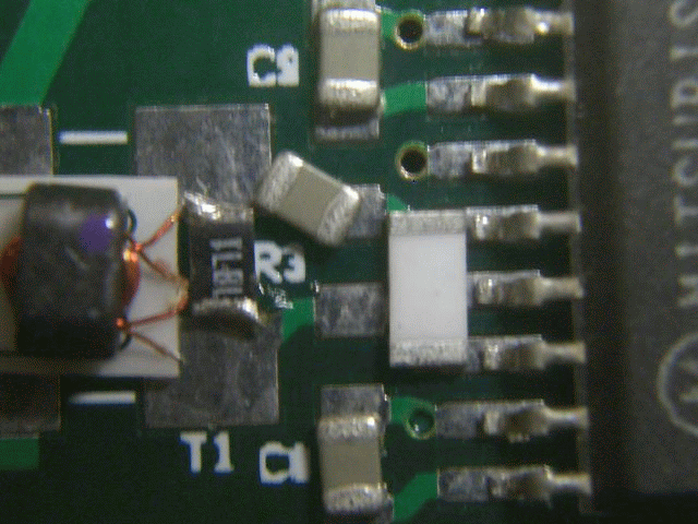
Use this drawing to order the pwb from Express, or use as Layout to locate the parts on the Board.
c.  PLSLIM-LD-8306 Rev A,  Parts List, maintained on this page, only.

    The SLIM-LD-8306 Log Detector has a dual function.  It is used as a logarithmic detector to convert RF power to DC voltage (RSSI).  And, it is used as a high gain, RF limited amplifier. The module has an input impedance of 50 ohms (J1) and a bandwidth of  3 MHz to 160 MHz.
   
The logarithmic dynamic range is -90 dBm to +10 dBm, with a DC output of +0.4 volts to +2.4 volts, on J2, "MAGVOLTS".  The module will respond to inputs above +10 dBm and below -90 dBm, but the output will not be logarithmic.
    The Limited I.F. Output (J3) is a 50 ohm source with 50 mv peak to peak, square wave output, with a duty cycle of 50/50.  The limiter input dynamic range is from -77 dBm to +10 dBm.
    It should be noted that this module is extremely sensitive to outside noise influence.  It is important that this module be totally shielded with a perimeter fence and a cover.

SK-PWB-LD-8306, Schematic of SLIM-LD-8306, Log Detector
slim/skslim_ld_8306.gif
    R3 is added to match the 1K ohm input impedance of the I.C. to the output impedance of the transformer.  The Limited I.F. Output, J3, is biased by R6 for a minimal output.  This will help prevent excessive feedback within the module that could induce self-oscillation.  The output is 50 mv peak to peak.  It can drive a high impedance or 50 ohm load.  If the Limited IF Output is not used, omit J3, R4, R5, R6, and C12.
    The bandwidth of this module is determined by the bandwidth of the input transformer.  The AD8306 has a much wider operating bandwidth.

Parts List, PLSLIM-LD-8306
Revision A,  5-18-2015 (updated 1-23-2016)
Des.     Value            Part Number.                                Digikey Number           Cost             Notes
C1        .1 uF            C0805C104K3RACTU                    399-1168-1-ND             0.05   
C2        .1 uF            C0805C104K3RACTU                    399-1168-1-ND       
     0.05   
C3        10uf/16v       TPSB106K016R0500                      478-5230-1-ND             0.65             Rev A
C4
        10uf/16v       TPSB106K016R0500                      478-5230-1-ND             0.65             Rev A
C5
          .1 uF            C0805C104K3RACTU                    399-1168-1-ND            0.05   
C6          .01 uF        C0805C103K5RACTU                      399-1158-1-ND            0.04       
C7
          .1 uF            C0805C104K3RACTU                    399-1168-1-ND            0.05   
C8          .1 uF            C0805C104K3RACTU                    399-1168-1-ND            0.05   
C9          .01 uF        C0805C103K5RACTU                      399-1158-1-ND            0.04       
C10        .1 uF            C0805C104K3RACTU                    399-1168-1-ND            0.05   
C11        .01 uF        C0805C103K5RACTU                      399-1158-1-ND            0.04       
C12        .01 uF        C0805C103K5RACTU                      399-1158-1-ND            0.04       
C13      .001 uF        ECJ-2VC1H102J                               PCC102CGCT-ND        0.08
FB1    Ferite Bead    BLM21PG221SN1D                        490-1054-1-ND              0.06
J1   
    SMA OPT        Molex, 538-73391-0070                WM5544-ND                 4.74   
J2        SMA OPT        Molex, 538-73391-0070                WM5544-ND                 4.74   
J3        SMA OPT        Molex, 538-73391-0070                WM5544-ND                 4.74   
P1    "Conn, 2 pin"    sold as row of 36 pins                       S1012E-36-ND               0.06    was S1012-36-ND
R1        10                MCR10ERTF10R0                       RHM10.0CHCT-ND          0.04    was MCR10EZHF10.0/RHM10.0CCT-ND 
R2        10                MCR10ERTF10R0                       RHM10.0CHCT-ND          0.04    was MCR10EZHF10.0/RHM10.0CCT-ND
R3        4.02K          MCR10ERTF4021                         RHM4.02KCCT-ND         0.04    was MCR10EZHF4.02K/RHM4.02KCCT-ND 
R4        49.9             MCR10ERTF49R9                       RHM49.9CHCT-ND          0.04    was MCR10EZHF49.9/RHM49.9CCT-ND
R5        49.9             MCR10ERTF49R9                       RHM49.9CHCT-ND          0.04    was MCR10EZHF49.9/RHM49.9CCT-ND
R6        390              MCR10ERTF3900                       RHM390CHCT-ND            0.04    was
MCR10EZHF390/RHM390CCT-ND
R7        2.7K            MCR10ERTF2701                       RHM2.70KCHCT-ND         0.04    was MCR10EZHF2.70K/RHM2.70KCCT-ND
T1    "Transf, 1:16"         TC16-161TG2+                      Minicircuits                       1.79
U1        78L05             78L05ACUTR                           497-1183-1-ND                 0.77
U2        AD8306           AD8306ARZ                            AD8306ARZ-ND              23.87
PWB    Circuit Board    PWB-LD-8306                                                                  3.28


PWB-LD-8306, Artwork for PWB and Layout for Log Detector, SLIM-LD-8306
slim/pwb_ld_8306.gif  slim/logdet.JPG
   
The input transformer could be replaced with other transformers, for different input impedances.  It could also be omitted and the transformer area used for an impedance matching network, for narrow band applications.

Input Impedance and Bandwidth
    The input impedance to this module is 50 ohms.  The input impedance to the AD8306 is 1000 ohms.  That is why the transformer is included.  It is a 1:4 turns ratio transformer.
  The voltage transformation ratio is 1:4, or 1 volt to 4 volts.  The impedance transformation ratio is 1:16, or 50 ohms to 800 ohms.  The power transformation is, of course, 1 to 1.  The 4.02 K (R3) shunt resistor is to decrease the total load resistance, on the secondary of the transformer, from 1000 ohms (the chip) to 800 ohms, for proper impedance matching.  The transformer is the factor for bandwidth limitation of 3 to 160 MHz. The following screen print is the Log Detector's Response to Input Power vs. Frequency.
msascreens/LogDetResp.gif

Dynamic Range
    Since the AD8306 has a high input impedance (1K ohm), Analog Devices uses voltage measurements (dBv) in their specification sheets, and not power measurements.  I am using power measurements (dBm) in the previous paragraphs, because I am specifying the inputs and outputs of the module itself, not the actual AD8306.  Once we move from the primary to the secondary, we are no longer in a 50 ohm system.  It is more accurate to use voltage measurements.
    As a reference point, let us assume the input voltage to the module (primary of transformer) is 1 volt rms, or 0 dBv (power = +13.03 dBm).  The output of the 1:4 transformer is 4 volts, or +12.04 dBv.  The transformer creates a voltage gain of 12.04 dB.  There is no power gain in a transformer.  Analog Devices specifies a logarithmic dynamic range of the AD8306 when its input is from -91 dBv to +9 dBv.  Since this is the secondary of the transformer, the dynamic range on the primary side, is -103.04 dBv to -3.04 dBv.  This equates to a 50 ohm power input of -90.01 dBm to +9.99 dBm.
    The Limiter amplifier of the AD8306 begins limiting at -78 dBv and remains stable to +9 dBv.  This equates to an input voltage on the primary side of the transformer of -90 dBv to -3 dBv.  As a 50 ohm input power to the module, this is -77 dBm to +10 dBm.
Below -77 dBm, the limiter output will become noisy (jitter) and the duty cycle will deviate from 50/50.
    If the Limiter Output of this module is never going to be used, it is advisable to omit components, R4, R5, R6, and C12.  This will lower power consumption and eliminate any possibility of limiter feedback oscillations.

Experimental Modification to
SLIM-LD-8306
   
8-05-2009   The duty cycle of the AD8306 limiter output is determined by the linearity of the input stage.  The AD8306 has internal biasing schemes to allow operation over a wide range of temperatures.  It is a fine design by Analog Devices.  But things could be better.  The input stage is not quite biased to its center, probably due to manufacturing tolerances.  I found that by changing the input bias, the output duty cycle can be maintained at 50/50, even when the input signal is close to the noise floor.
    This is how I found the input level vs. output duty cycle relationship.  Connect the Limiter Output (J3) to a 50 ohm loaded oscilloscope.  Inject a 10.7 MHz signal on the input (J1).  Adjust the input signal power level to somewhere between 0 dBm and -40 dBm.  The duty cycle is very close to 50/50.  Gradually, decrease the input power and notice that the duty cycle will change with decreasing input power.  It will become extreme as the input signal approaches the lower limit of the Limiter's dynamic range.  This can be improved with a modification to "skew" the bias on one input to the I.C.
    This is the modification.
slim/logdetmod.gif
    Power down, remove lid, and perform the following steps.
1.  Reposition R3 to the output pads of T1 to allow for the remaining mods.
2.  Cut and create a gap in the trace between U2 pin 4 and T1
3.  Install a .01 ufd chip capacitor across the gap.
4.  Obtain a chip resistor of 470 K ohms to 1 Meg ohms. Call this Rx. A size 1206 is perfect.
5.  Power up and repeat the previous duty cycle test.
6.  Adjust the input power to a level where the duty cycle is obviously not 50/50
7.  Position Rx from U1 pin 4 to ground.  U1 pin 6 is a very convenient ground pin.
8.  If the duty cycle moves in the direction of 50/50 or completely passes it, this is the correct position for the final location of our trim resistor.  If the duty cycle becomes worse, then the correct position for Rx will be from U1 pin 5 to pin 7.
9.  Use an exacto knife or something to grind off all the resist from Rx, leaving only the ceramic substrate and solderable ends.  Notice, in the photo, Rx is much cleaner than you will achieve (I cheated).
10. Power down and permanently mount Rx in the correct position.
11. Power up and repeat the
duty cycle test.
12.
Adjust the input power to a level where the duty cycle is obviously not 50/50
13. Use a pencil and make a mark from one end of Rx to the other.  The duty cycle should move back toward 50/50.  If it passes 50/50 the pencil carbon is too conductive.  Clean Rx with alcohol and try again with a different pencil.  You are now creating a resistor with very high resistance.  The more carbon you mark onto Rx, the less the total resistance.
14.  Decrease the input power and the duty cycle should become worse, in the same direction.  Add more pencil carbon to bring the duty cycle back toward 50/50.
15.  Continue decreasing power, and adding carbon, until you are at the point where the duty cycle looks extremely noisy but still maintaining 50/50.  You may temporarily place the lid on the top of the module to decrease some of this noise while testing.
16.  If you add too much carbon, clean it all off with alcohol and a brush and start over.
17.  When you are happy with this tweeking process, power down and drop a drop of Q-Dope over Rx.  Do not brush it on, as this will disturb the carbon tracks and change the resistance.  Dope will prevent humidity from changing the value of Rx and upsetting the new bias point.  A good substitute for dope is CLEAR nail polish.  Yes, I am yelling.  DO NOT USE colored nail polish.  Let it dry.  Do not use nail polish that is water soluble.
18.  After drying, repeat
the duty cycle test.  If it has changed significantly, scrape off the dope and start over.
    This modification is very touchy and is not necessary for MSA applications.  It is just that I like to play with things and see if they can be improved.  In this case, not only did the duty cycle improve, but the Log output of the device also improved.  The noise floor decreased and allowed more dynamic range.  I love this stuff.
    Here is another thing to play with. You may be able to extend the Dynamic Range of the Module a few dB with extra cooling.  The minimum measurable input to the Module is approximately -90 dBm.  This equates to the noise floor of the 8306.  However, I have found that by lowering the ambient temperature of the 8306, its noise floor decreases. With a lower noise floor, it will respond to inputs less than -90 dBm.  I used an ice cube in a plastic baggie and placed it on the bottom of the Module.
The ambient temperature of the I.C. went from about 90 degrees F to (guessing) 32 degrees F. The noise floor dropped significantly.  How much? Well, as a guess, I think the noise floor dropped about 5 dB, allowing a signal measurement improvement of about 3 dB. One suggestion I received: install a Peltier Cell on the bottom of the Module, directly under where the 8306 is located.  Peltier Cells are power hogs but it would be fun to play with.  To use this idea, I would think that the Module would have to be fully sealed to prevent condensation inside the module.
    I am using this Log Detector Module in the MSA. I am using a muffin fan to keep the MSA from getting too warm. I purposely positioned the fan to blow outside air directly on the Log Detector Module to keep it as cool as possible.