PWB-RFA rev 0
Dual RF Amplifier Board
Released 7-01-07,  original pwb release date, but this is a new web page, published 2-9-2011.

PWB-RFA, Printed Wiring Board, Dual RF Amplifier, size-A
Use your mouse's "right click" and "Save Link" to download:
a.
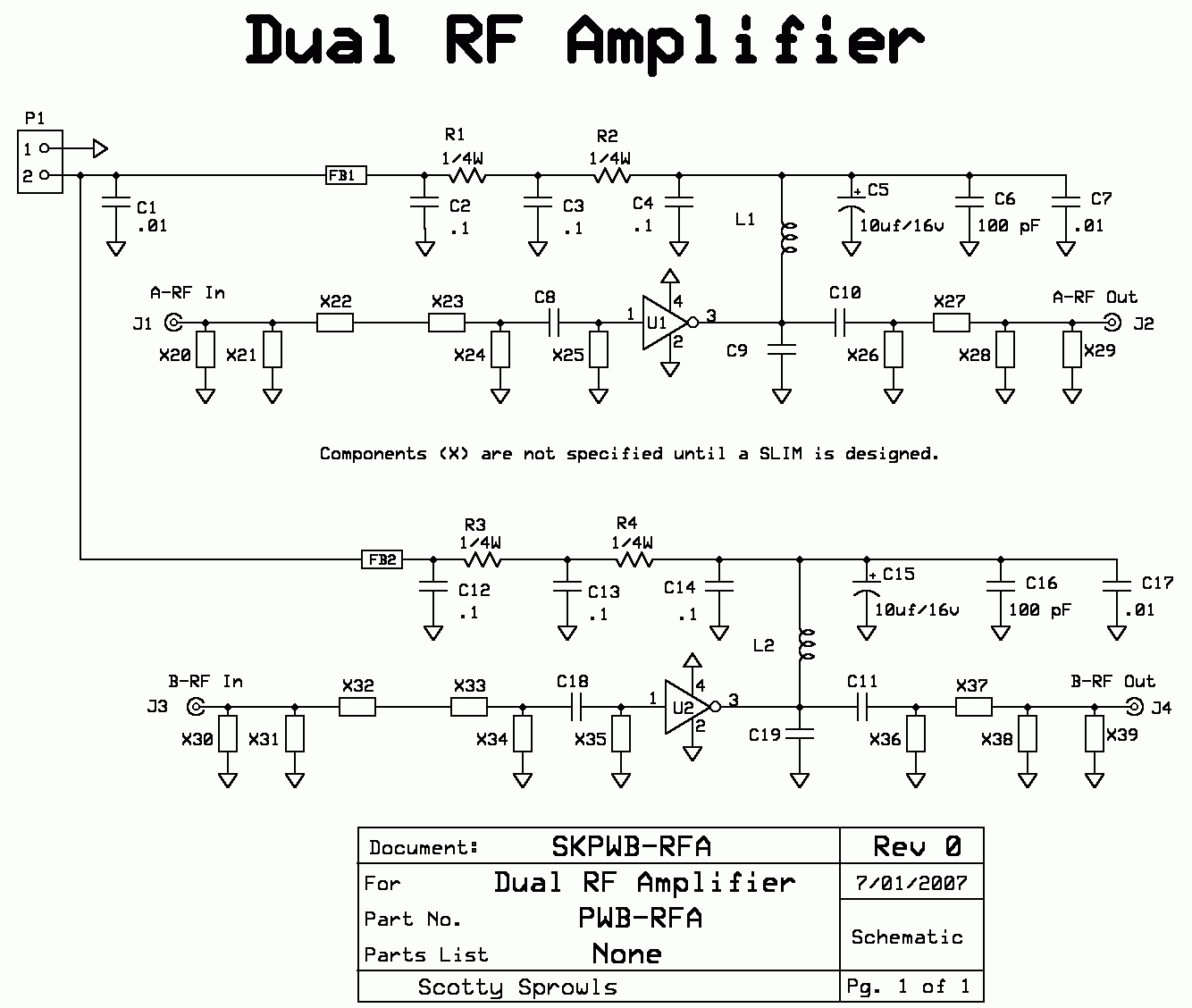
  No schematic is released for this pwb. However, a general purpose schematic is shown on this page.
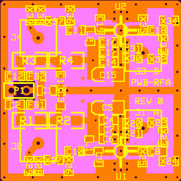
b.  No layout is released for this pwb. However, a component layout is shown on this page for locating parts on board.
c.   PWB-RFA, PWB artwork, in ExpressPCB software. Use for ordering from Express.
d.   No parts list is released for this pwb. A module that uses this PWB will have its own PL.

    The Dual RF Amplifier PWB can accomodate two separate MMIC amplifiers with a common DC power input connector.  Any MMIC amplifier can be used that has a "footprint" that will fit this pwb.

General Schematic of PWB-RFA. Not released, but shown here.
slim/skpwb_rfa.gif
    Only the The U1 side (A side) of the Dual Amplifier is described. The mirror components on the U2 side perform the identical functions.
*  C1, FB1, C2, R1, and C3 perform low pass filtering for the voltage source input.
The total resistance of R1, R2 and L1 determine the operating current for U1.
*  The supply voltage shown is +10 volts, but can be changed if R1 and R2 are re-calculated.
C4, C5, C6, and C7 provide a low impedance ground source for the output signal.
L1 provides the DC voltage source coupling for the MMIC, U1. It should present a minimum reactance that is about 500 ohms within the bandwidth of the amplifier. However, L1 can be replaced with a resistor, and will act as part of an output attenuator. R1 and R2 can be adjusted, accordingly. This is useful for very low frequency or very broad band applications.
Input Circuit:
X20, X21, X22, X23, X24, C8, and X25 can be any type of components to form a passive circuit. Such as, attenuator, low pass filter, band pass filter, or high pass filter. Usually, MMIC amplifiers must have their inputs AC coupled (DC blocked), with no DC biasing or ground resistance. If so, X25 cannot be a resistor or inductor. C8 is usually the DC blocking capacitor for the MMIC. Its value can be adjusted so that it is part of the input circuit.
Output Circuit:
C9, C10, X26, X27, X28, and X29 can be any type of components to form a passive circuit. Such as, attenuator, low pass filter, band pass filter, or high pass filter. DC biased MMIC amplifiers must have their outputs AC coupled (DC blocked) to the load circuits. If so, C9 cannot be a resistor or inductor and C10 is usually a capacitor. C10 is usually the DC blocking capacitor for the MMIC. Its value can be adjusted so that it is part of the output circuit.

PWB-RFA, Layout, Top (Component) View
slim/pwb_rfa.gif
    This layout can be used for locating or placement of components.  All component positions are shown. However, most applications will not use all of the components. Connectors J1-J4 and P1 are mounted on the bottom side, ground plane of the PWB. Size is 1.2 inch x 1.2 inch.