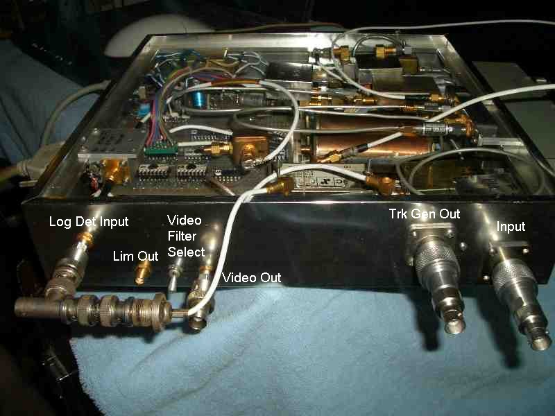
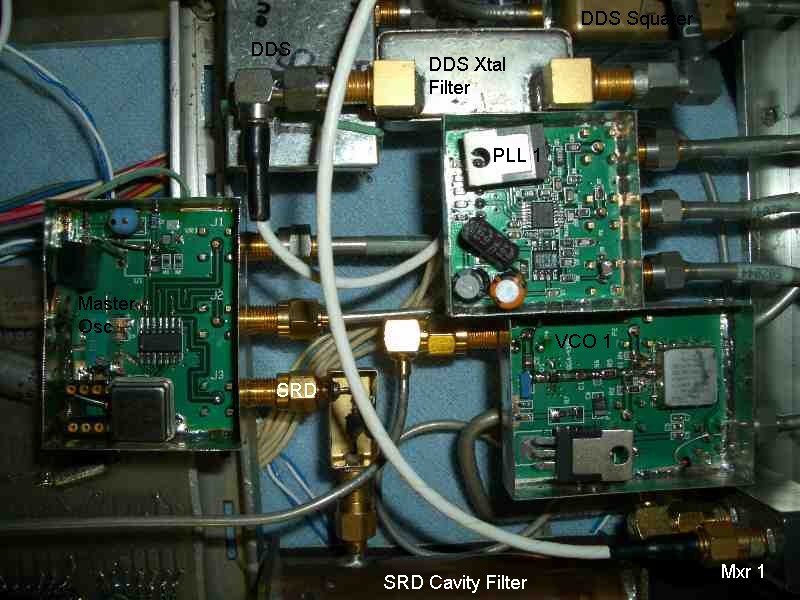
Page for Original
Modularized Spectrum Analyzer
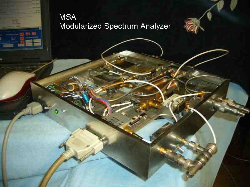
The
original MSA mated with a laptop computer. Not pretty, but works
quite well.
This Site was Started Jan. 02, 2004
Updated this page Sept. 1, 2007
11-01-09 This page is no longer maintained.
This Page, for the Original MSA, will present construction ideas for the Basic Spectrum Analyzer, using Modular Construction. Other pages support the operation, and software for the Modularized Spectrum Analyzer, including modifications to the Basic MSA to include a Tracking Generator. More (in-work) pages show how to convert the MSA/Tracking Generator to a Vector Network Analyzer (MSA/VNA).
Here are other links supporting this original MSA :
Tracking Generator Addition page for the MSA.
Operation and Calibration page for the MSA. Instructions for calibration and alignment.
Testing the Modules page for the MSA. Instructions for testing individual modules.
Software page for the MSA. Description of the software code.
Link to Builder's Group for those interested in sharing ideas on the MSA. There are several people in the process of building the MSA and can offer suggestions and comments. This is a Yahoo Group page and you are welcome to enter and contribute.
MSA as a Vector Network Analyzer. An in-work page to convert the MSA into a high frequency VNA. Note that, this page is in-work and there is much to be added.
Coaxial Cavity Bandpass Filter. A page for construction of the MSA bandpass filter.
Step Recovery Diode frequency multiplier scheme that can replace LO 2 in the MSA
These are the operating Specifications of the original MSA:
Dual Conversion 1013.3 MHz first I.F., 10.7 MHz final I.F.
Frequency Response 2 KHz to 1140 MHz (with 2 KHz resolution bandwidth filter)
Min. Step Freq. Response 1.4 Hz at 0 Mhz, 2.8 Hz at 1000 MHz
Input Power Sensitivity -20 dBm to -110 dBm
Maximum Power Input +17 dBm or 40 milliamps (without damage)
Dynamic Range > 90 dB
Amplitude Resolution Appx 0.03 dB
Selectivity (BW) I use 4 different Final I.F. BW filters: 9.5 MHz/200 Hz, 11.15 Mz/2 KHz,
10.695 MHz/4 KHz, 10.7 MHz/15 KHz
Noise Figure 24 dB
Phase Noise -97 dBc/Hz (1 Hz BW), 3 KHz away from carrier
-97 dBc/Hz 10 KHz away from carrier
-89 dBc/Hz 40 KHz away from carrier (noise peaking)
-101 dBc/Hz 100 KHz away from carrier
-114 dBc/Hz 300 KHz away from carrier
better than -116 dBc/Hz 500 KHz away from carrier or above
Image Rejection In-Band Image Rejection is better than -112 dBc,
IM Distortion Two tone, better than -60 dBc, worse case. Avg better than -70 dBc
Other Hardware Required:
PC or Laptop Computer with LPT 1 standard parallel port. Windows 95 or later.
Monitor can be any size, but must be set for a minimum of 800 by 600 pixel resolution. More is fine.
I am using a Toshiba Satellite Laptop, 700 MHz Celeron.
Software Required
Application software is Liberty Basic 3.01 or more recent. I am not a software guru. I was famaliar only with HP Basic and Commodore Basic and this is very similar. Liberty is also very inexpensive, their trial version 4.0 is free. Go visit their web site at www.libertybasic.com.
Description of the MSA:
Block Diagram for 0 to 1 GHz MSA

I built the Modularized Spectrum Analyzer using modular techniques, with SMA connectors and RG-141 or RG-085 hard pipe interconnecting the modules. Most of the modules were built using printed circuit boards supplied by Cash Olsen. A few others were built "dead bug" style or substituted with connectorized components.
Each module, except the Control Module, must be totally shielded to prevent stray RF interference. I use a 1/2 to 1 inch tall "fence" cut from coffee can lids, placed around the perimeter of the module's pwb and soldered on both sides of the board. I formed a lid from the same material, so that it fit over the top of each module. After testing is complete, the lids can be soldered to the fence.
I have some general design and construction guidelines for modules that are susceptible to RF interference. They are:
Do not have a pad, line trace, or component pin exposed to the outside of the module unless it is well bypassed (decoupling capacitors). For example, mount DIP packages in a surface mount style, and don't allow the pins to stick through the board.
Each module should contain its own voltage regulator. This will maintain good power regulation for the devices, and it will also help contain RFI within the module.
RF inputs and outputs of each module can be either SMA (or any small connector) or directly soldered, coaxial cable. I have been quite successful with direct connections using RG-188. Click here to view a method of Coaxial Direct Connection to a PCB. I have gone so far as to remove the outer insulation and "sweat" the outer braid with solder. This makes a 100% outer jacket. Almost as good as hard pipe!
Module Descriptions:
Mixer 1 and Mixer 2 Modules
There are a many mixers that will perform well at the intended frequencies of the MSA. For best response at very low input frequencies, I used the "I" port of mixer 1 as the input to the MSA. I must caution the builder that some commercial mixers are not as they are advertised. That is, my definition of an "I port" is the port that is coupled to the diode network, not the transformer network. The diode network port usually has a much better low frequency response than the R or L ports. MSA inputs down to a few KHz can be measured quite accurately, depending on the quality of Mixer 1. If the mixer has a very good L port to I port isolation (greater than 40 dB), input frequencies as low as the bandwidth of the Final IF Xtal Filter can be measured. One more caution: the I port of a mixer can be destroyed by a high level input signal. Good rule of thumb to prevent mixer damage: maximum input signal should not be greater than the specified LO input power. And NEVER, apply DC voltage to any port of a mixer, this could result in destruction of the mixer.
In my current MSA, I am using a connectorized Watkins Johnson M1J for Mxr 1. For Mxr 2, I am using an ERSL-38X. They can be substituted with a variety of other mixers. Any +7 dBm or +13 dBm drive mixer that has an IF port response from DC to 1000 MHz can be used. The RF port should have a good response at 1000 MHz and the LO port should have good response from 1000 MHz to 2000 MHz. For Mixer 1, choose a mixer that has the best interport isolation. 40 dB isolation from L to R (or better) would be great. For building your own Mixer Module, the following is a viable alternative.
Generic Mixer Module using ADE-11X:
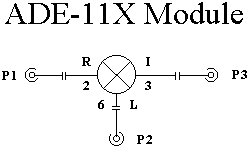
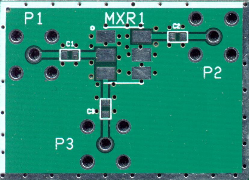
This mixer module is shown with coupling capacitors on each port. In reality, they are not always needed. However, the spacing is there in case the builder would like to add blocking capacitors, a resistive pi network attenuator, or a pi type filter using descrete components. Note that the port markings are per Minicircuits specifications. In reality, pins 3 and 6 are the transformer inputs and pin 2 is the diode bridge. The ADE-11X is not the most optimum mixer because it has poor L to R port isolation at 1013 MHz (-24 dB). However, it does have less conversion loss than the specs, closer to 6.0 dB, and is very inexpensive. This pwb was done by Cash Olsen at www.zianet.com/erg and can be used for any mixer that has the same footprint as the ADE-11X.

Here are suggested designs for Mixer 1 and Mixer 2 for the MSA. The attenuators are designed for -6 dB. If different attenuation (or none) is required, simply change the resistor networks. Mixer 2 is designed with a low pass filter, to attenuate high level frequency products before entering the I.F. amplifier. Note: The I port in the schematic is the mixer port with the diodes.
1013.3 MHz First Intermediate Frequency Filter :
The main purpose of the first I.F. filter is to attenuate the in-band image frequency, which is at 1034.7 MHz. There are some pretty good, high Q filter designs out there. Don't be afraid to substitute. For example, my present MSA is using an Interdigital Filter that was found on e-bay and supplied to me from Bruce, in Canada. The following is my design of a Coaxial Cavity Filter that has extremely good selectivity. It was built and tested in the MSA, giving an attenuation of -112 dBc at 1034 MHz. It has a loaded Q of over 500.
First I.F. Coaxial Cavity Filter :
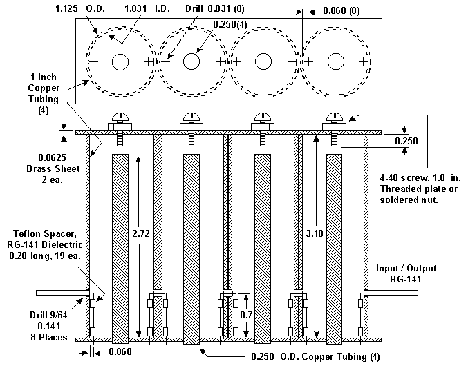
I must tell you, plumbing is not my "thing", but, this was really easy to build. I used RG-141 hardpipe for input and output. I disected some RG-141 to use its center conductor for interstage "hairpin" coupling and use it's teflon dielectric for spacers. It was "fairly" close to 50 ohms and had a loss of about 7 dB. Silver plating would improve insertion loss but, hey, let's keep it cheap. Besides, loss is not a concern here. Depending on the length of the tuning screws, this filter will tune from 800 MHz to 1150 MHz. The bandwidth should be about 2 MHz. I bought the copper tubing at Home Depot in a 24" length. I took my measurements with me and used their pipe cutter. I used .062 brass for the end plates and threaded one for the tuning screws. Thinner material would require soldering a 4-40 nut on the material to hold the tuning screws. For my in-band Image frequency measurements, this filter performed brilliantly. Image was better than -112 dBc. See more on how to construct a cavity filter : Cavity Filter Construction Page
VCO Modules :
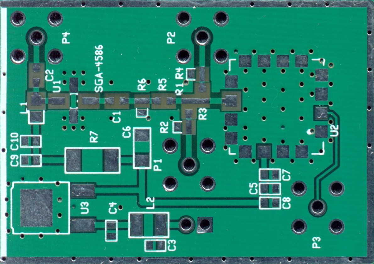
A Voltage Controlled Oscillator, in combination with a PLL, is used for each Local Oscillator in the MSA. LO 1 frequency range is 1013.3 MHz to 2013.3 MHz. LO 2 is a fixed frequency of 1024 MHz. These frequencies assume that the MSA has a first I.F. frequency of 1013.3 MHz and a Final I.F. frequency of 10.7 MHz. LO 2 can be replaced by an optional frequency multiplier scheme. The following is a generic schematic and layout for any VCO that uses the footprint of the Minicircuits ROS type of VCO. The output is high enough to drive a high level mixer (+13 dBm). It should be padded down to about +7 for driving standard level mixers. The resistors in the padding networks for P1 and P2 can be recalculated for other values of attenuation. The pwb, shown, was produced by Cash Olsen.
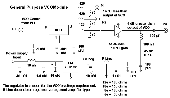
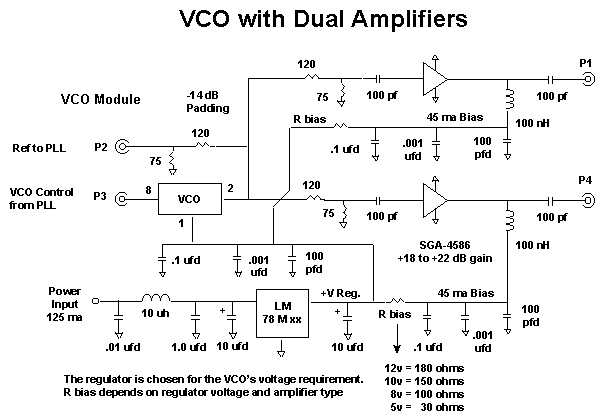
Updated 9-22-06 The following is a schematic of a General Purpose VCO Module with dual buffer amplifier outputs. I recommend using this circuit when adding a Tracking Generator or converting the MSA into a Vector Network Analyzer. I actually modified the above PWB to accomodate the second amplifier, but I don't recommend this operation for the squeemish!
VCO 1 Module using ROS-2150VW :
This VCO uses a Vcc of +5v. Therefore the regulator should be an LM78M05 and the R bias resistor should be 30 ohms. It will tune from 950 MHz to 2200 MHz. Output of the amplified port (P4) is about +8 dBm.
VCO 1 Module using UMS-2150-R16 :
This VCO uses a Vcc of +12v. Therefore the regulator should be an LM78M12 and the R bias resistor should be 180 ohms. It will tune from 900 MHz (.6v), 1500 MHz (6.5v), to 2300 MHz (17.5v). Output of the P4 is about +13 dBm. My present MSA is utilizing the UMS-2150 for VCO 1.
VCO 1 Module using V585ME08 :
This VCO specifies a Vcc of 10v. However, I built up this module using a Vcc of +12v, to increase the VCO output power. Therefore the regulator should be an LM78M12 and the R bias resistor should be 180 ohms. It will tune from 960 MHz to 2300 MHz . Output of the P4 is about +13 dBm.
VCO 2 Module using ROS-1500 :
This VCO uses a Vcc of +10v. Therefore the regulator should be an LM78M10 and the R bias resistor should be 150 ohms. It will tune from 990 MHz (1v), 1100 MHz (5v), and 1024 MHz (2.5v).This tuning characteristic is perfect for matching with a non-amplified (direct) PLL.
VCO 2 Module using V583ME01 :
This VCO uses a Vcc of +5v. Therefore the regulator should be an LM78M05 and the R bias resistor should be 30 ohms. It will tune from 700 MHz (.1v), 1024 MHz (4.35v), to 1300 MHz (9.0v). My present MSA is utilizing the V583ME01 for VCO 2.
PLL Modules :
There are many PLL integrated circuits that will work quite well in the MSA. These module designs integrate a PLL chip and it's loop components in it's own module, separate from the VCO component. That way, mixing and matching components for specific frequency generation is as easy as changing modules. There are two types of PLL modules discussed here. The PLL, Type 1 style has an active amplifier in it's loop filter. The PLL Type 2 style is a direct loop, that is, no amplifier.
If a VCO will provide the correct output frequency when it's tuning voltage is within the output voltage range of the PLL integrated circuit, then no amplification is required. This is the PLL Type 2 style and is used for the MSA's LO 2.
In the MSA, the VCO 1 requires about +18 volts to tune to the highest frequency. Since a PLL IC cannot supply more than +5 volts, an amplifier is required in the Loop Filter. The PLL Tye 1 style Module uses an op-amp as an amplifier. The OP27 has been an industry standard for low noise, PLL loop amplifiers, for many years. There are new op amps that will work quite well, in place of the OP27. These include (but are not limited to) LT1677, AD8610, AD8510, AD8033, AD8671, and AD8065. I am using the last two in my present MSA/VNA.
The software I have written for the MSA will accomodate 5 different PLL's (at this time). They are the National LMX 2325, LMX 2326, LMX 2350, LMX 2353, and Analog Devices AD 4112.
PLL Type 1, using LMX 2326 or ADF 4112: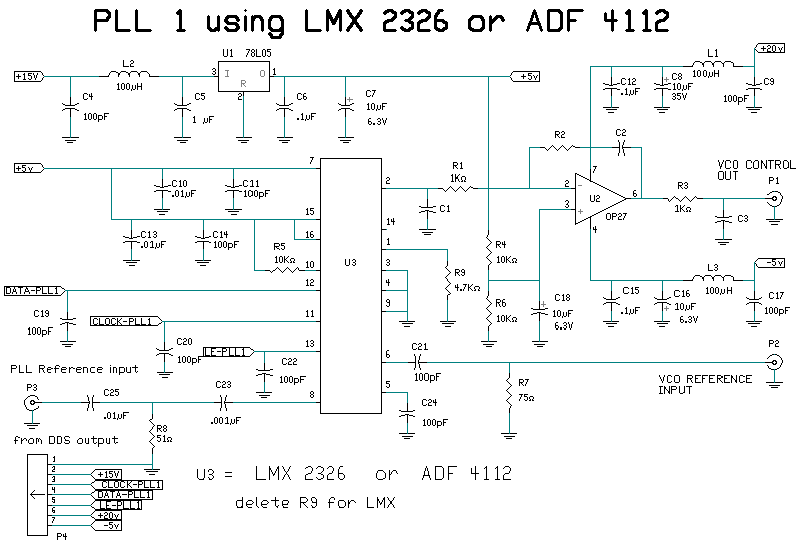
PLL 1 schematic, using LMX 2326 or ADF 4112
This PLL board was produced by Cash Olsen
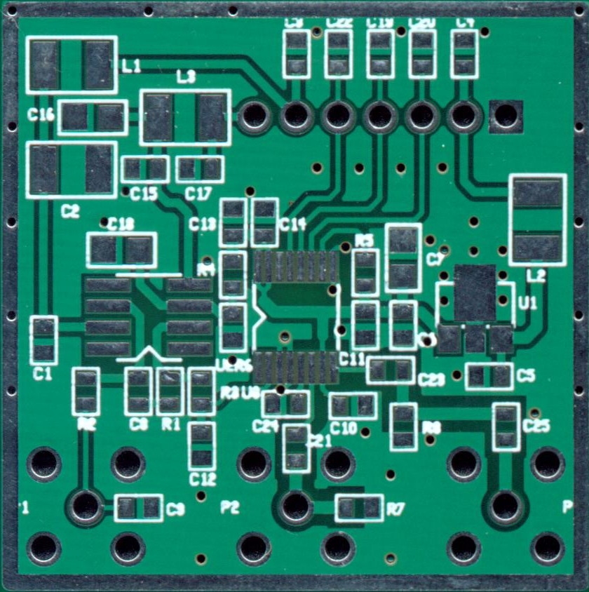
This module schematic and board design will except the LMX 2326 or ADF 4112. If using the LMX, delete the R9, 4.7 K. The operating characteristics of the ADF is different, but is commanded, in software, to look electrically identical to the LMX 2326. This module can also be used as PLL 2 in the MSA if the builder opts for a VCO that requires an op amp.
C1, R2, C2, and C3 are values that determine the Loop Response of the PLL. These values depend on the PLL charge pump current and the operating Phase Detector Frequency (PDF). For minimum PLL phase noise, the PDF is usually chosen to be as high as possible, but is limited by several factors:
1. The minimum N-Divider ratio within the PLL. For example, the LMX 2326 minimum N division ratio is 992. With a minimum VCO 1 frequency of 1013 MHz, the PDF cannot be greater than 1.02 MHz.
2. The DDS output frequency and it's associated filter bandwidth. The wider the filter bandwidth, the higher a PDF can be attained. For example: The DDS output and center frequency of the DDS filter is 10.7 MHz. The filter has a bandwidth of 15 KHz. This is the formula that determines the maximum PDF that can be used for a particular DDS output frequency:
PDF = Bandwidth of DDS filter x minimum VCO Frequency / Center Frequency of DDS Filter.
In this case: PDF = .015 MHz x 1013 MHz / 10.7 MHz = 1.42 MHz. If using an LMX 2326, the maximum PDF is 1.02 MHz, due to it's minimum N counter. Try using 1.02 MHz as a PDF. Determine the R divider ratio of the PLL, that is the division ratio of the Reference input frequency to the PDF =
DDS output frequency / PDF = 10.7 MHz / 1.02 MHz = 10.49. This is not possible since the division ratio must be a whole number. It must be chosen to be 11, since 10 would give a PDF higher than the limitation of the PLL's minimum N counter of 992. Therefore, the PDF will be 10.7 MHz / 11 = .9727 MHz. This is the frequency at which the PLL 1 Loop filter should be designed.
For a 7.5 KHz bandwidth filter, the maximum PDF is = .0075 x 1013 / 10.7 = .71 MHz. The divider ratio would be 10.7 / .71 = 15.07 using 16. Therefore, the PDF would be .66875 MHz. A divider ratio of 15 would give a PDF of .7133 MHz , within the limitation of the LMX 2326 N-counter, but too great a frequency shift to remain within the bandwidth of the DDS filter.
For a 4.5 KHz bandwidth filter, the maximum PDF is = .004 x 1013 / 10.7 = .379 MHz. The divider ratio would be 10.7 / .379 = 28.25 using 29. Therefore, the PDF would be .369 MHz.
Here are some suggested component values to use in the loop filter for PLL 1. The values are dependent on the operating Phase Detector Frequency (PDF), Charge Pump Current (Icp) and the VCO's tuning gain. They will also, determine close-in phase noise, noise peaking, and lock time. They can be modified at the descretion of the builder. Determining Loop Filter components is not an easy task. I use, and suggest the experimentor download, a really nice (and free) PLL program called ADI SimPLL. It can be downloaded at the Analog Devices Web Site. It uses the ADF type PLLs for models, but you can "fudge" the parameters to make them look like LMX devices. The following numbers for PLL 1 assume the VCO is a ROS-2150VW, or UMS-2150 (70 MHz/volt).
PLL 1 Used as Icp PDF C1 R2 C2 C3
LMX2326 IntegerN 1.0 ma .669 MHz 220 pf 10.0 K 680 pf 820 pf
ADF 4112 IntegerN 5.0 ma .669 MHz 220 pf 2.0 K 3.3 nf 820 pf
LMX2325 IntegerN 5.0 ma .669 MHz 220 pf 2.0 K 3.3 nf 820 pf
LMX2350/53 IntegerN 1.6 ma .669 MHz 220 pf 6.2 K 1.0 nf 820 pf
LMX2326 IntegerN 1.0 ma .973 MHz 180 pf 10 K 470 pf 560 pf
LMX2326 IntegerN 1.0 ma .973 MHz 100 pf 2 K 10 nf 5 nf (my present MSA)
LMX2326 IntegerN 1.0 ma .369 MHz 470 pf 10.0 K 1.2 nf 1.5 nf
Click here to see a schematic of PLL 1 using the LMX 2353.
PLL Type 2 style, using LMX 2326 or ADF 4112:
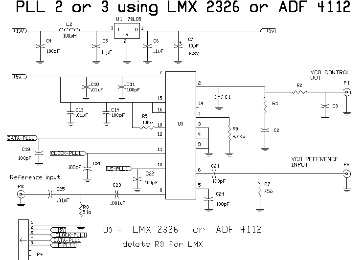
PLL 2 using LMX 2326 or ADF 4112
This pwb was done by Cash Olsen
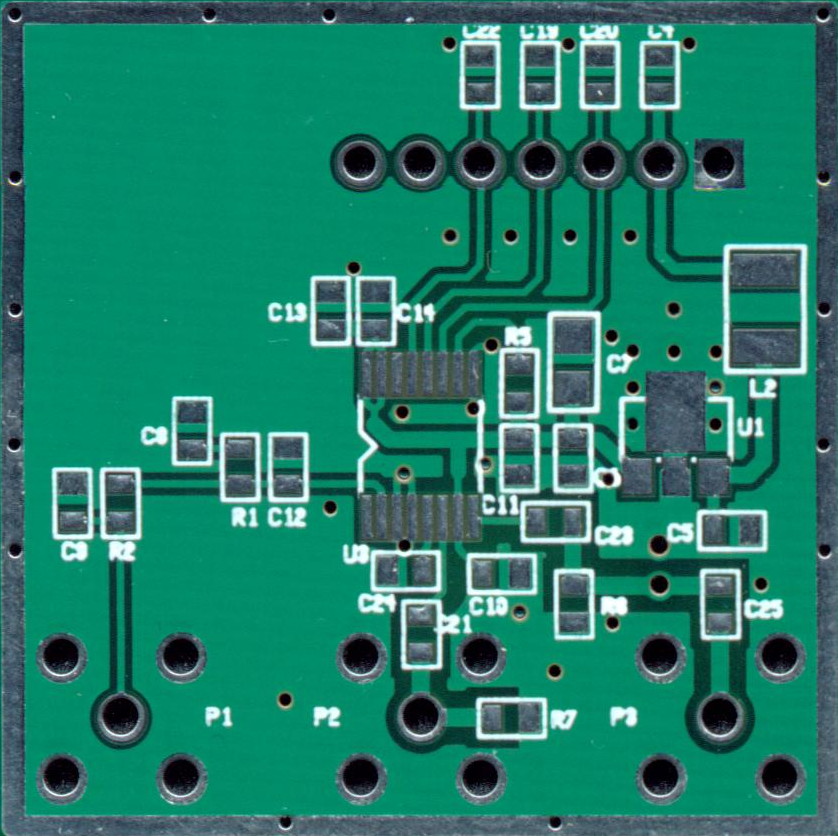
This module is the same basic schematic and layout as the PLL 1 module, but with the op amp area deleted. I suggest running the Phase Detector Frequency at 4 MHz for PLL 2.
Here are some suggested component values for the PLL 2 loop filter. The values are dependent on the operating Phase Detector Frequency (PDF), Charge Pump Current (Icp) and the VCO's tuning gain. They will also, determine close-in phase noise, noise peaking, and lock time. They can be modified, at the descretion of the builder. These values assume the VCO is an ROS-1500 (26 MHz/volt).
PLL 2 Used as Icp PDF C1 R1 C2 R2 C3
LMX2326 IntegerN 1.0 ma 4.0 MHz 180 pf 2.7 K 8.2 nf 2.2 K 270 pf
LMX2326 IntegerN 1.0 ma 4.0 MHz 1 nf 1 K 15 nf 1 K 1 nf (present MSA)
LMX2350/53 IntegerN 1.6 ma 4.0 MHz 220 pf 2.2 K 10.0 nf 2.2 K 270 pf
LMX2325 IntegerN 5.0 ma 4.0 MHz 680 pf 680 33.0 nf 2.2 K 270 pf
ADF 4112 IntegerN 5.0 ma 4.0 MHz 680 pf 680 33.0 nf 2.2 K 270 pf
Final I.F. Amplifier :
Any linear amplifier with gain at 10.7 MHz can be used for the Final IF amplifier. It should be capable of a +10 dBm output, without compression. The noise figure should be 3 dB or less. The amount of amplification is optional with the builder. With MSA mixer and filter losses totaling, approximately, -24 dB, an amplifier with a gain of about 44 dB is suggested. I will present two modularized amplifiers here, a single stage and a 3 stage amplifier.
Single Amplifier using ERA-33SM or SGA-4586 :
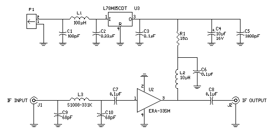
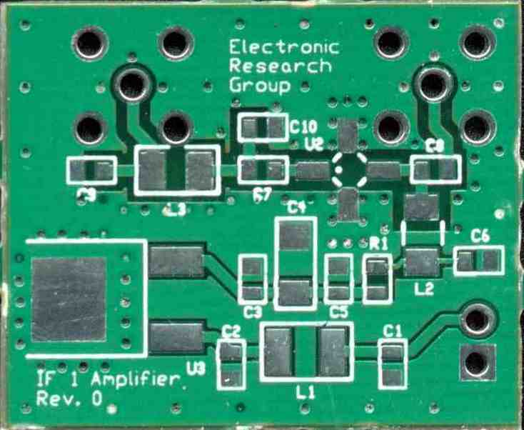 This
single stage amplifier has a gain of about 19.5 dB at 10.7 MHz.
The ERA-33SM amplifier can be replaced with an SGA-4586 or other such
"pill" amplifier. The bias resistor, R1, must be changed to the
proper value for other amplifiers. For an SGA-4586,
the value would be 30 ohms and the gain would be approximately 29 dB at
10.7 MHz. The pi type filter (C9, C10, L3) does not
need to be populated if
this amplifier is not intended to be used as the MSA's first final I.F.
amplifier.
This pwb was done by Cash Olsen
This
single stage amplifier has a gain of about 19.5 dB at 10.7 MHz.
The ERA-33SM amplifier can be replaced with an SGA-4586 or other such
"pill" amplifier. The bias resistor, R1, must be changed to the
proper value for other amplifiers. For an SGA-4586,
the value would be 30 ohms and the gain would be approximately 29 dB at
10.7 MHz. The pi type filter (C9, C10, L3) does not
need to be populated if
this amplifier is not intended to be used as the MSA's first final I.F.
amplifier.
This pwb was done by Cash Olsen
3 Stage Amplifier using ERA-33SM or SGA-4586 :

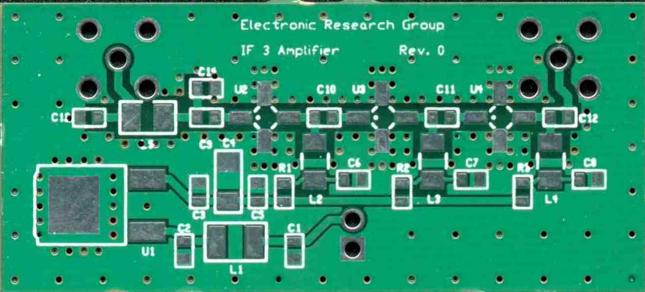 This 3 single
stage amplifier has a gain of about 58 dB at 10.7 MHz. The
ERA-33SM
amplifiers can be replaced with SGA-4586 or other such "pill"
amplifiers. The bias resistor, R1-R3, must be changed to the
proper values
for other amplifiers. For an SGA-4586, the value would
be 30 ohms and the gain would be approximately 87 dB at 10.7 MHz.
This would be way too much gain for the MSA. Populate
the board with only two SGA-4586 amplifiers and the total
gain will be about 58 dB.
This pwb was done by Cash Olsen
Final I.F. Xtal Filter :
The Final Xtal Filter determines the Resolution Bandwidth of the MSA. Steep slopes and out of band rejection is a must for good selectivity. A single filter can be designed and placed here, giving the MSA a single resolution BW. The software is written to allow up to 4 different filters that can be placed in circuit, for a multiple resolution BW spectrum analyzer. I would suggest using filters with the following bandwidths: 200 Hz, 2 KHz, 15 or 30 KHz, and 300 KHz. I have found that a 2 KHz BW filter is a very good general purpose.
The above section, Dynamic Range of the MSA, explains the effect of wide band noise on the MSA. If the builder prefers a very wide band filter (greater than 15 KHz) I suggest he decrease the gain of the amplifier to allow for best dynamic range.
If you want to design your own crystal filter, there are numerous crystal filter design programs, but I find that a very good (and free) one is AADE Filter Design. I have version 4.03. You might check the AADE Website for his latest update. There are numerous surplus crystal filters that can be found on the internet. In many cases, they are already connectorized and matched for 50 ohms. There is no hard rule that the frequency of the Final filter has to be 10.7 MHz. I have used several crystal filters from my junk box: 9.954 MHz/2KHz BW, 10.695 MHz/4KHz, 11.15 MHz/2KHz, 10.7 MHz/15KHz, 10.7 MHz/30 KHz. Crystal filter input/output impedances vary quite a bit, but range in the 300 ohm to 2000 ohm area. The matching network shown below, can be a good starting point. Once the analyzer is built and tested, the matching values can be tweeked to get good results using the "self testing" capability of the Analyzer, itself, (narrow sweep around 0 MHz). I would suggest downloading the free RFSim99 software. It has automatic impedance matching circuits within. Try these sites for downloads:
http://doppler.unl.edu/~rockee/summer_2003/RFSim99.exe
http://www.sandiego.edu/~ekim/e194rfs01/RFSim99.exe
Here is a 10.695 MHz crystal filter taken from an old CB radio. It has 4 internal monolithic crystal filters. It has a bandwidth of 2.6 KHz and is easily matched to 50 ohms:

Log Detector Module :
The Log Detector is the mechanism for converting RF power to a dc voltage. Be aware that this, and any, log detector is very responsive to broad band frequencies, and noise. The Log Det Module must be preceeded by a bandwidth limiting filter.
Log Detector using MC3356 :
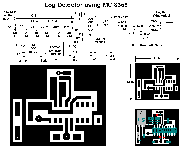
Although this device is no longer manufactured, It can be found in many surplus devices. I find it very "friendly" when constructing this module "dead bug" style, since it is a standard DIP package. It also has an RF Limited output, although very high impedance. I am using it it the MSA/VNA conversion.
It has a dynamic range of -90 dBm to 0 dBm, although linearity is poor in the highest and lowest 10 dB or range. The output slope ranges from .27 volts to 2.75 volts. There is an error on the schematic, change C2 from .1 uf to 1.0 uf.
Log Detector using AD8307 :
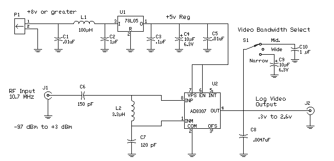
For an input of -97 dBm to +3 dBm at 10.7 MHz, the resulting output slope is about 400 millivolts to 2.4 volts. It has excellent log linearity between -90 dBm and 0 dBm, with a log response of about 20 mv/dB. No post video amplification is necessary, since the 12 bit analog to digital converter on the control board responds nicely to these levels.
Notice that the input does not have a 50 ohm resistive load. The input impedance of the 8307 is 1.1 K ohms. Therefore, I designed a matching circuit, 50 ohms source to 1.1 k load at 10.7 MHz. This has an effective voltage gain and requires less drive to achieve full scale output. I have not built this circuit. It is a "blind" design effort, but I have built and tested the following AD 8306 circuit, which is similar.
Log Detector using AD8306 :
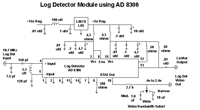
The AD8306 has similar characteristics as the AD8307, and it has a limited RF output. The limiter is not used in the MSA, but I chose this device so that I would have a "sampled" I.F. when expanding the MSA into a Vector Network Analyzer. For an input of -90 dBm to +10 dBm at 10.7 MHz, the resulting output slope is about 400 millivolts to 2.4 volts. It has excellent log linearity between -85 dBm and +10 dBm, with a log response of about 20 mv/dB.
DDS using AD9850 : Click on schematic to enlarge and see detail.
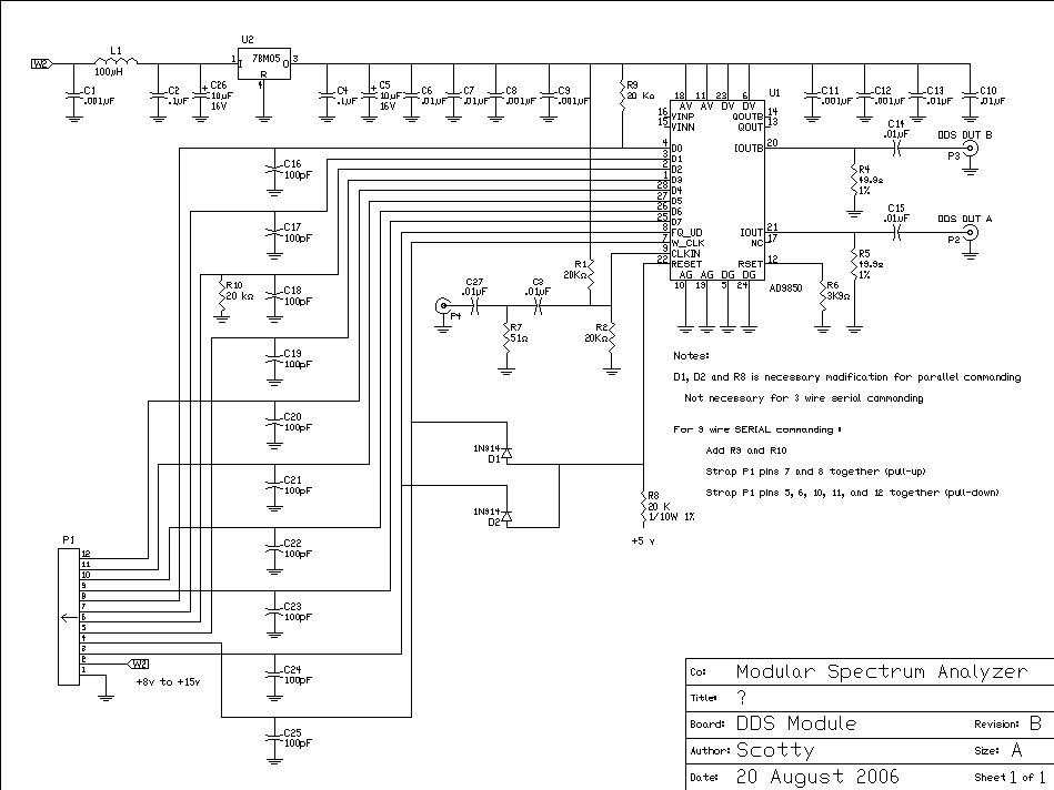
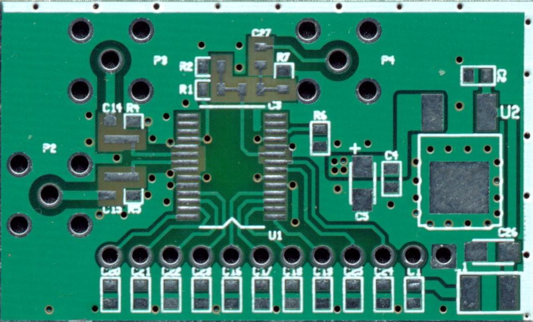
This DDS Module is the steering mechanism for the PLL 1 Module (LO 1) in the Modularized Spectrum Analyzer. It is used as a Clock Source for the PLL 1. In effect, the output of the DDS will be multiplied N times, by PLL 1, to create the actual frequency of LO 1.
There are 2 output ports for this DDS design. The extra port can be used at the descretion of the builder. When the spare port is not used, connect a 50 ohm load to the port.
On June 13, 2005 I added a modification that will allow the software to "Reset" the DDS using the WCLK and FQUD lines as an "and" function. There can be a strange computer situation where, upon power up, the DDS might "hang-up" in a strange function. When running the MSA software (revision 103 or later), there is an automatic Reset that will prevent this occurance. This DDS pwb was produced by Cash Olsen. A hardware modification to this board, is the addition of D1, D2, and R9. The DDS reset pin-22 was at ground. Remove pin-22 from ground and connect to the diode anodes. Connect the diode cathodes to P1, pins 3 and 4. Connect one end of resistor R9 to the anodes and the other end to +5v.
The DDS output will have an amplitude of approximately -8 dBm at 10.7 MHz. The signal will also contain alias frequencies and many spurious frequencies. The output of the DDS must be well filtered, to eliminate spurious and alias frequencies, before using it as a steering clock for PLL 1. A crystal filter is the best choice for this function. They are plentiful, cheap, and easy to incorporate (see DDS Xtal Filter Module). I have chosen the DDS output to be 10.7 MHz, since this filter frequency is the most plentiful. It is not a requirement for the DDS to operate with an output of 10.7 MHz. Normally, I would advise that the DDS output frequency not be within the bandwidth of the Final IF filter. However, I have built three spectrum analyzers with both frequencies being the same, and had no problem. Good shielding of the modules plays an important role in preventing the DDS output from getting into the Final IF modules.
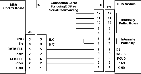
On August 20, 2006 I added a modification to allow the DDS Module to be commanded serially by 3-wire control. The modification consists of adding a 20 K ohm resistor from P1 pin 8 to +5v. A second 20 K ohm resistor is added from P1 pin 6 to ground. This modification will not effect the module when it is commanded in parallel mode, from the Control Board J5. This modification is necessary when connecting the DDS Module to the Control Board J4. The following diagram is for an interconnection cable, from Control Board J4 to DDS Module P1, to allow a DDS Module to be serially commanded. (Added 10-18-06)
DDS Xtal Filter Module :
You may have seen DDS designs that use a low pass filter on the output. These wide filters are necessary to utilize the maximum capability of the DDS. In the MSA, the DDS frequency is only changed about 7 KHz. With this narrow bandwidth, a crystal filter is a logical choice for filtering the DDS.
Selection of the Xtal Filter Bandwidth is a compromise in the MSA. We would like to have the bandwidth of this filter to be very narrow, to attenuate the alias and spur frequencies that are created by the DDS. On the other hand, we need it wide enough to allow the DDS to "steer" the PLL 1 module as much as possible to allow a high Phase Detector Frequency in PLL 1. The bandwidth of this DDS filter will determine the maximum phase detector frequency of the PLL 1 module.
There are two very common 10.7 MHz crystal filters, with bandwidths of 7.5 KHz and 15 KHz. Either one can be used in the MSA. The narrower 7.5 KHz will allow fewer spurious, and the wider 15 KHz will allow a lower overall phase noise in the MSA. Either of these filters could be utilized and their outputs taken directly to the PLL 1. The filtered output level is enough to use as a Reference Clock for PLL 1. However, PLL 1 phase noise can be improved by as much as 3 dB, by squaring the DDS Xtal Filter output signal. The squaring circuit could be placed within the DDS Xtal Filter Module, or placed in line, externally. The following design is a combination and will accomodate any crystal filter.
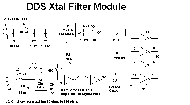
The Schematic is a general purpose design for any Monolithic Crystal Filter. The values of the components, L2, C8, and R1 are nominal. They depend on the actual impedance characteristics of the MCF. This design is for a 500 ohm input/output impedance. The 74AC04 has a great deal of gain, and when biased to its center, will function well for low input level sine waves. The use of this module, in the MSA, is to square up the 10.7 MHz output of the DDS to drive the PLL 1 Module. With no input, this circuit will, most likely, oscillate, so don't let that fool you. Do not be tempted to use the spare gates of the '04 for any other purpose.
Control Board Module :
Updated 3-14-06. I have made some changes to the Control Board that will give the builder more options on how to incorporate an AtoD converter. The change is, schematically removing the integrated AtoD converter from the Control Board. The builder then has the option to construct the AtoD circuit directly onto the Control Board, or construct the AtoD as an external module. The following are the options for the builder:
Control Board with integrated 8 Bit A/D, this is the original design.
Control Board with integrated 12 Bit A/D, this is an upgrade of the original design.
Control Board with integrated 16 Bit Serial A/D. This is the latest design, using an Analog Devices IC.
Control Board with external A/D Module with a connection cable.
If you have already built one of the previous Control Boards, don't worry. The latest software version will handle all of the options. You will notice that each option has dual A/D conversion. The Phase AtoD is represented, but may be ommitted. The presently designed MSA uses only the Magnitude AtoD. The Phase A/D is there to use when I finalize the MSA as a Vector Network Analyzer.
This is the new schematic of the MSA Control Board, RevA :
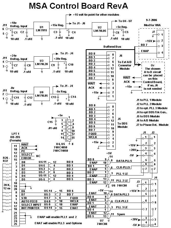
The Control Board is the Interface between the home computer and the Modularized Spectrum Analyzer's modules. U4 and U5 buffer the Computer's parallel port input (LPT 1), to allow a "hot swap". The addition of J6 allows connections to an external AtoD Module. Of course, the AtoD can be integrated directly onto the Control Board and J6 is not needed.
Updated 9-7-06. Add J7 connector for VNA upgrade. This modification is not necessary for the basic MSA, or MSA with Tracking Generator.
Analog to Digital Converter Modules :
The following AtoD designs can be built as a module, or can be integrated directly onto the Control Board. If integrated, the on-board 5v regulator circuit is not needed.
8 Bit A to D Converter :
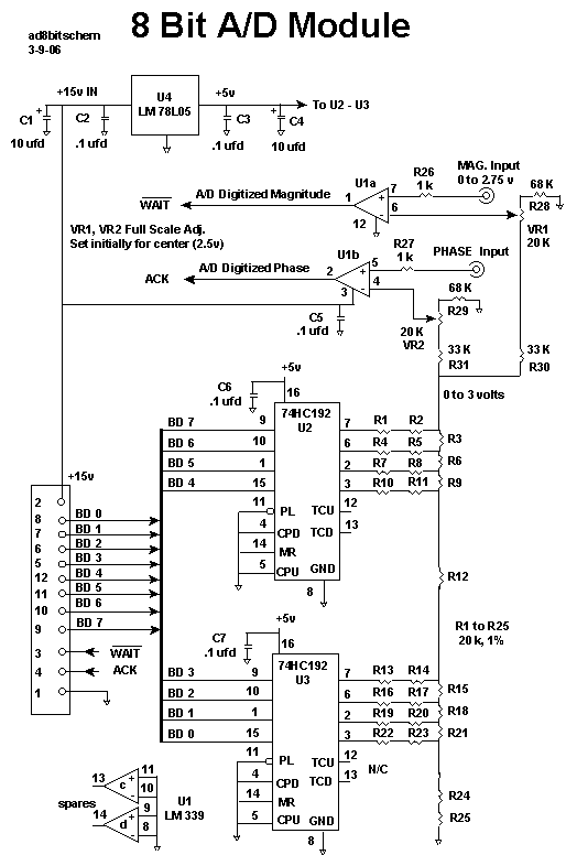
The A to D is really an analog to analog comparator. The computer program does the itterations that a manufacturer's A to D chip would do by itself. The 8 bits of data supplied by the computer code is converted to an analog voltage by U2 and U3 and compared (at U1) to the voltage created by the Log Detector Module. U2 and U3 are used as buffers, and any 74HC series buffer could have been used. Use the best precision resistors possible in the ladder network. Use an ohmmeter and measure a whole bunch of same value resistors, and select 25 that are the closest to each other. 20 K ohms is a nominal value, but you can use any value from 10K to 22K ohms. The better the resistor tolerance, the better the log linearity will be. Don't settle for worse than 1% difference in the ladder network. To maintain the proper ladder resistance, the combination of resistors R28-R31 and VR1 and VR2 must present a total load to the ladder output point (R2, R3), that is exactly 3 times the value of ladder resistor used. In this case, 3x20K=60 K ohms. 8 Bit conversion will give the MSA an amplitude resolution of about 0.3 dB. Click here to open the original schematic of the Control Board with integrated 8 Bit AtoD.
12 Bit A to D Converter :
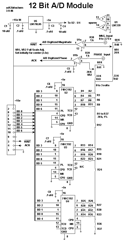
Just as in the 8 Bit Converter, the software commands U2, U3, and U4 to act like a Successive Approximation Analog to Digital Converter. Here, 4 bits of data supplied by the computer code is converted to an analog voltage by U2, U3 and U4 and compared to the voltage created by the Log Detector Module. U2, U3 and U4 are used as a data latch, and any 74HC series latch could have been used. To maintain the proper ladder resistance, the combination of resistors R40-R43 and VR1 and VR2 must present a total load to the ladder output point (R2, R3), that is exactly 3 times the value of ladder resistor used. In this case, 3x20=60 K ohms. Since 12 bits will allow up to 4095 steps of resolution, the amplitude resolution is about .03 dB. Click here to open the original schematic of the Control Board with 12 Bit DtoA.
16 Bit Serial A to D Converter :
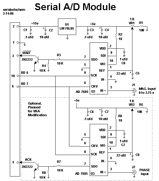
The software commands U2, U3 to begin conversion with a single toggle of bit BD7. Subsequent toggles of bit BD6 causes SCK to output a serial stream of 16 bits. Both A/D's can capture, and can then clock out their data concurrently. The software will read these bits on the WAIT and ACK lines. 16 bits will allow up to 65,536 steps of resolution. The 2 least significant bits are somewhat noisy which yields, a more realistic, 14 bit resolution. Therefore, with this scheme, the amplitude resolution of the MSA is about .01 dB.
Master Oscillator Module :
I have designed the Master Oscillator into its own module, because, many builders may want to use their own oscillator designs. There are 3 modules in the MSA that require a Master Clock signal: The DDS, PLL 2, and PLL 3 (Tracking Generator, if installed).
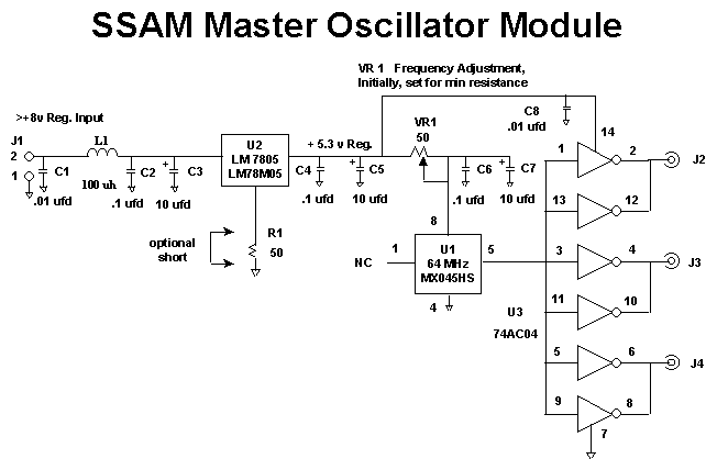
This Master Oscillator Module is designed for maximum utility. The oscillator is buffered with a 74AC04 and has 3 outputs. Each output will drive a 50 ohm load, but I suggest the load be capacitively coupled to reduce power consumption in the buffer. If any output is not used, leave it open.
The CTS, MX045 is chosen because I have had very good success with this inexpensive oscillator. It is quite stable after a few minutes of warm up; however, it will not be exactly on frequency. Therefore, I designed a "cheating" way to set the frequency. The oscillator will push in frequency with a minor change of Vcc. The voltage regulator is biased with the 50 ohm resistor and its output will be approximately 5.3 volts. Construct the module with R1 in place, but with a small shorting wire across R1. Adjust VR 1 for minimum resistance and check the frequency. If you can adjust VR 1 to bring the frequency to exactly 64 MHz, leave the short on R1. If not, open the short and adjust VR1 for exact frequency. For example, one of my tests showed that the 5v reg. was outputting 5.11 volts with the short. The osc was at 64.000697 MHz. Adjusting VR 1 for 5.01 volts on the MXO oscillator gave exactly 64.000000 MHz. If the builder is not planning to add the optional Tracking Generator, the Master Oscillator Frequency does not need to be adjusted. The software will allow frequency intolerance.
I have found that when the module is totally enclosed, the frequency becomes quite stable after about 5 minutes. However, with the module open, any air currents will cause temperature changes on the MXO oscillator, and cause frequency shifts.
Note that, if the R1 is left in circuit, the tab of the voltage regulator is NOT at ground potential and must be isolated from ground.
Optional Tracking Generator :
Updated 8-26-06. I removed the information for the tracking generator portion and moved in to it's own page. Go here to see Tracking Generator.
Power Supply :
I do not show a design for a power supply. Any Linear supply will work. DO NOT use any form of switching supply. This analyzer is REALLY sensitive and will pick up any switching noise. The voltage regulators are on the Control Board. Required input voltages are +24 v @ approx. 10 ma; +18 v to +24 v @ approx. 300 ma; and -8 v to -20 v @ approx. 10 ma. I should emphasize that good power supply filtering and active component bypassing is very important. This MSA is quite sensitive to very low input power levels and any extraneous power supply noise can effect measurements.
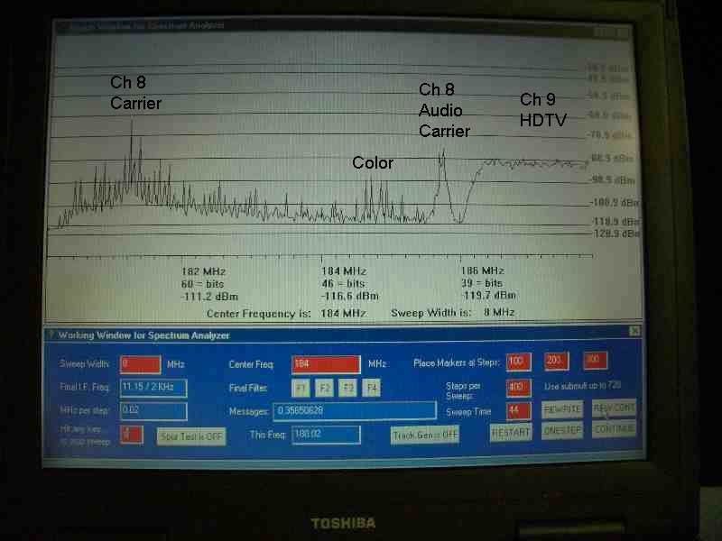
Graph and Working Window :
This Site was Started Jan. 02, 2004
Updated this page Sept. 1, 2007
11-01-09 This page is no longer maintained.
This Page, for the Original MSA, will present construction ideas for the Basic Spectrum Analyzer, using Modular Construction. Other pages support the operation, and software for the Modularized Spectrum Analyzer, including modifications to the Basic MSA to include a Tracking Generator. More (in-work) pages show how to convert the MSA/Tracking Generator to a Vector Network Analyzer (MSA/VNA).
Here are other links supporting this original MSA :
Tracking Generator Addition page for the MSA.
Operation and Calibration page for the MSA. Instructions for calibration and alignment.
Testing the Modules page for the MSA. Instructions for testing individual modules.
Software page for the MSA. Description of the software code.
Link to Builder's Group for those interested in sharing ideas on the MSA. There are several people in the process of building the MSA and can offer suggestions and comments. This is a Yahoo Group page and you are welcome to enter and contribute.
MSA as a Vector Network Analyzer. An in-work page to convert the MSA into a high frequency VNA. Note that, this page is in-work and there is much to be added.
Coaxial Cavity Bandpass Filter. A page for construction of the MSA bandpass filter.
Step Recovery Diode frequency multiplier scheme that can replace LO 2 in the MSA
These are the operating Specifications of the original MSA:
Dual Conversion 1013.3 MHz first I.F., 10.7 MHz final I.F.
Frequency Response 2 KHz to 1140 MHz (with 2 KHz resolution bandwidth filter)
Min. Step Freq. Response 1.4 Hz at 0 Mhz, 2.8 Hz at 1000 MHz
Input Power Sensitivity -20 dBm to -110 dBm
Maximum Power Input +17 dBm or 40 milliamps (without damage)
Dynamic Range > 90 dB
Amplitude Resolution Appx 0.03 dB
Selectivity (BW) I use 4 different Final I.F. BW filters: 9.5 MHz/200 Hz, 11.15 Mz/2 KHz,
10.695 MHz/4 KHz, 10.7 MHz/15 KHz
Noise Figure 24 dB
Phase Noise -97 dBc/Hz (1 Hz BW), 3 KHz away from carrier
-97 dBc/Hz 10 KHz away from carrier
-89 dBc/Hz 40 KHz away from carrier (noise peaking)
-101 dBc/Hz 100 KHz away from carrier
-114 dBc/Hz 300 KHz away from carrier
better than -116 dBc/Hz 500 KHz away from carrier or above
Image Rejection In-Band Image Rejection is better than -112 dBc,
IM Distortion Two tone, better than -60 dBc, worse case. Avg better than -70 dBc
Other Hardware Required:
PC or Laptop Computer with LPT 1 standard parallel port. Windows 95 or later.
Monitor can be any size, but must be set for a minimum of 800 by 600 pixel resolution. More is fine.
I am using a Toshiba Satellite Laptop, 700 MHz Celeron.
Software Required
Application software is Liberty Basic 3.01 or more recent. I am not a software guru. I was famaliar only with HP Basic and Commodore Basic and this is very similar. Liberty is also very inexpensive, their trial version 4.0 is free. Go visit their web site at www.libertybasic.com.
Description of the MSA:
Block Diagram for 0 to 1 GHz MSA

I built the Modularized Spectrum Analyzer using modular techniques, with SMA connectors and RG-141 or RG-085 hard pipe interconnecting the modules. Most of the modules were built using printed circuit boards supplied by Cash Olsen. A few others were built "dead bug" style or substituted with connectorized components.
Each module, except the Control Module, must be totally shielded to prevent stray RF interference. I use a 1/2 to 1 inch tall "fence" cut from coffee can lids, placed around the perimeter of the module's pwb and soldered on both sides of the board. I formed a lid from the same material, so that it fit over the top of each module. After testing is complete, the lids can be soldered to the fence.
I have some general design and construction guidelines for modules that are susceptible to RF interference. They are:
Do not have a pad, line trace, or component pin exposed to the outside of the module unless it is well bypassed (decoupling capacitors). For example, mount DIP packages in a surface mount style, and don't allow the pins to stick through the board.
Each module should contain its own voltage regulator. This will maintain good power regulation for the devices, and it will also help contain RFI within the module.
RF inputs and outputs of each module can be either SMA (or any small connector) or directly soldered, coaxial cable. I have been quite successful with direct connections using RG-188. Click here to view a method of Coaxial Direct Connection to a PCB. I have gone so far as to remove the outer insulation and "sweat" the outer braid with solder. This makes a 100% outer jacket. Almost as good as hard pipe!
Module Descriptions:
Mixer 1 and Mixer 2 Modules
There are a many mixers that will perform well at the intended frequencies of the MSA. For best response at very low input frequencies, I used the "I" port of mixer 1 as the input to the MSA. I must caution the builder that some commercial mixers are not as they are advertised. That is, my definition of an "I port" is the port that is coupled to the diode network, not the transformer network. The diode network port usually has a much better low frequency response than the R or L ports. MSA inputs down to a few KHz can be measured quite accurately, depending on the quality of Mixer 1. If the mixer has a very good L port to I port isolation (greater than 40 dB), input frequencies as low as the bandwidth of the Final IF Xtal Filter can be measured. One more caution: the I port of a mixer can be destroyed by a high level input signal. Good rule of thumb to prevent mixer damage: maximum input signal should not be greater than the specified LO input power. And NEVER, apply DC voltage to any port of a mixer, this could result in destruction of the mixer.
In my current MSA, I am using a connectorized Watkins Johnson M1J for Mxr 1. For Mxr 2, I am using an ERSL-38X. They can be substituted with a variety of other mixers. Any +7 dBm or +13 dBm drive mixer that has an IF port response from DC to 1000 MHz can be used. The RF port should have a good response at 1000 MHz and the LO port should have good response from 1000 MHz to 2000 MHz. For Mixer 1, choose a mixer that has the best interport isolation. 40 dB isolation from L to R (or better) would be great. For building your own Mixer Module, the following is a viable alternative.
Generic Mixer Module using ADE-11X:


This mixer module is shown with coupling capacitors on each port. In reality, they are not always needed. However, the spacing is there in case the builder would like to add blocking capacitors, a resistive pi network attenuator, or a pi type filter using descrete components. Note that the port markings are per Minicircuits specifications. In reality, pins 3 and 6 are the transformer inputs and pin 2 is the diode bridge. The ADE-11X is not the most optimum mixer because it has poor L to R port isolation at 1013 MHz (-24 dB). However, it does have less conversion loss than the specs, closer to 6.0 dB, and is very inexpensive. This pwb was done by Cash Olsen at www.zianet.com/erg and can be used for any mixer that has the same footprint as the ADE-11X.

Here are suggested designs for Mixer 1 and Mixer 2 for the MSA. The attenuators are designed for -6 dB. If different attenuation (or none) is required, simply change the resistor networks. Mixer 2 is designed with a low pass filter, to attenuate high level frequency products before entering the I.F. amplifier. Note: The I port in the schematic is the mixer port with the diodes.
1013.3 MHz First Intermediate Frequency Filter :
The main purpose of the first I.F. filter is to attenuate the in-band image frequency, which is at 1034.7 MHz. There are some pretty good, high Q filter designs out there. Don't be afraid to substitute. For example, my present MSA is using an Interdigital Filter that was found on e-bay and supplied to me from Bruce, in Canada. The following is my design of a Coaxial Cavity Filter that has extremely good selectivity. It was built and tested in the MSA, giving an attenuation of -112 dBc at 1034 MHz. It has a loaded Q of over 500.
First I.F. Coaxial Cavity Filter :

I must tell you, plumbing is not my "thing", but, this was really easy to build. I used RG-141 hardpipe for input and output. I disected some RG-141 to use its center conductor for interstage "hairpin" coupling and use it's teflon dielectric for spacers. It was "fairly" close to 50 ohms and had a loss of about 7 dB. Silver plating would improve insertion loss but, hey, let's keep it cheap. Besides, loss is not a concern here. Depending on the length of the tuning screws, this filter will tune from 800 MHz to 1150 MHz. The bandwidth should be about 2 MHz. I bought the copper tubing at Home Depot in a 24" length. I took my measurements with me and used their pipe cutter. I used .062 brass for the end plates and threaded one for the tuning screws. Thinner material would require soldering a 4-40 nut on the material to hold the tuning screws. For my in-band Image frequency measurements, this filter performed brilliantly. Image was better than -112 dBc. See more on how to construct a cavity filter : Cavity Filter Construction Page
VCO Modules :
A Voltage Controlled Oscillator, in combination with a PLL, is used for each Local Oscillator in the MSA. LO 1 frequency range is 1013.3 MHz to 2013.3 MHz. LO 2 is a fixed frequency of 1024 MHz. These frequencies assume that the MSA has a first I.F. frequency of 1013.3 MHz and a Final I.F. frequency of 10.7 MHz. LO 2 can be replaced by an optional frequency multiplier scheme. The following is a generic schematic and layout for any VCO that uses the footprint of the Minicircuits ROS type of VCO. The output is high enough to drive a high level mixer (+13 dBm). It should be padded down to about +7 for driving standard level mixers. The resistors in the padding networks for P1 and P2 can be recalculated for other values of attenuation. The pwb, shown, was produced by Cash Olsen.


Updated 9-22-06 The following is a schematic of a General Purpose VCO Module with dual buffer amplifier outputs. I recommend using this circuit when adding a Tracking Generator or converting the MSA into a Vector Network Analyzer. I actually modified the above PWB to accomodate the second amplifier, but I don't recommend this operation for the squeemish!

VCO 1 Module using ROS-2150VW :
This VCO uses a Vcc of +5v. Therefore the regulator should be an LM78M05 and the R bias resistor should be 30 ohms. It will tune from 950 MHz to 2200 MHz. Output of the amplified port (P4) is about +8 dBm.
VCO 1 Module using UMS-2150-R16 :
This VCO uses a Vcc of +12v. Therefore the regulator should be an LM78M12 and the R bias resistor should be 180 ohms. It will tune from 900 MHz (.6v), 1500 MHz (6.5v), to 2300 MHz (17.5v). Output of the P4 is about +13 dBm. My present MSA is utilizing the UMS-2150 for VCO 1.
VCO 1 Module using V585ME08 :
This VCO specifies a Vcc of 10v. However, I built up this module using a Vcc of +12v, to increase the VCO output power. Therefore the regulator should be an LM78M12 and the R bias resistor should be 180 ohms. It will tune from 960 MHz to 2300 MHz . Output of the P4 is about +13 dBm.
VCO 2 Module using ROS-1500 :
This VCO uses a Vcc of +10v. Therefore the regulator should be an LM78M10 and the R bias resistor should be 150 ohms. It will tune from 990 MHz (1v), 1100 MHz (5v), and 1024 MHz (2.5v).This tuning characteristic is perfect for matching with a non-amplified (direct) PLL.
VCO 2 Module using V583ME01 :
This VCO uses a Vcc of +5v. Therefore the regulator should be an LM78M05 and the R bias resistor should be 30 ohms. It will tune from 700 MHz (.1v), 1024 MHz (4.35v), to 1300 MHz (9.0v). My present MSA is utilizing the V583ME01 for VCO 2.
PLL Modules :
There are many PLL integrated circuits that will work quite well in the MSA. These module designs integrate a PLL chip and it's loop components in it's own module, separate from the VCO component. That way, mixing and matching components for specific frequency generation is as easy as changing modules. There are two types of PLL modules discussed here. The PLL, Type 1 style has an active amplifier in it's loop filter. The PLL Type 2 style is a direct loop, that is, no amplifier.
If a VCO will provide the correct output frequency when it's tuning voltage is within the output voltage range of the PLL integrated circuit, then no amplification is required. This is the PLL Type 2 style and is used for the MSA's LO 2.
In the MSA, the VCO 1 requires about +18 volts to tune to the highest frequency. Since a PLL IC cannot supply more than +5 volts, an amplifier is required in the Loop Filter. The PLL Tye 1 style Module uses an op-amp as an amplifier. The OP27 has been an industry standard for low noise, PLL loop amplifiers, for many years. There are new op amps that will work quite well, in place of the OP27. These include (but are not limited to) LT1677, AD8610, AD8510, AD8033, AD8671, and AD8065. I am using the last two in my present MSA/VNA.
The software I have written for the MSA will accomodate 5 different PLL's (at this time). They are the National LMX 2325, LMX 2326, LMX 2350, LMX 2353, and Analog Devices AD 4112.
PLL Type 1, using LMX 2326 or ADF 4112:

PLL 1 schematic, using LMX 2326 or ADF 4112
This PLL board was produced by Cash Olsen

This module schematic and board design will except the LMX 2326 or ADF 4112. If using the LMX, delete the R9, 4.7 K. The operating characteristics of the ADF is different, but is commanded, in software, to look electrically identical to the LMX 2326. This module can also be used as PLL 2 in the MSA if the builder opts for a VCO that requires an op amp.
C1, R2, C2, and C3 are values that determine the Loop Response of the PLL. These values depend on the PLL charge pump current and the operating Phase Detector Frequency (PDF). For minimum PLL phase noise, the PDF is usually chosen to be as high as possible, but is limited by several factors:
1. The minimum N-Divider ratio within the PLL. For example, the LMX 2326 minimum N division ratio is 992. With a minimum VCO 1 frequency of 1013 MHz, the PDF cannot be greater than 1.02 MHz.
2. The DDS output frequency and it's associated filter bandwidth. The wider the filter bandwidth, the higher a PDF can be attained. For example: The DDS output and center frequency of the DDS filter is 10.7 MHz. The filter has a bandwidth of 15 KHz. This is the formula that determines the maximum PDF that can be used for a particular DDS output frequency:
PDF = Bandwidth of DDS filter x minimum VCO Frequency / Center Frequency of DDS Filter.
In this case: PDF = .015 MHz x 1013 MHz / 10.7 MHz = 1.42 MHz. If using an LMX 2326, the maximum PDF is 1.02 MHz, due to it's minimum N counter. Try using 1.02 MHz as a PDF. Determine the R divider ratio of the PLL, that is the division ratio of the Reference input frequency to the PDF =
DDS output frequency / PDF = 10.7 MHz / 1.02 MHz = 10.49. This is not possible since the division ratio must be a whole number. It must be chosen to be 11, since 10 would give a PDF higher than the limitation of the PLL's minimum N counter of 992. Therefore, the PDF will be 10.7 MHz / 11 = .9727 MHz. This is the frequency at which the PLL 1 Loop filter should be designed.
For a 7.5 KHz bandwidth filter, the maximum PDF is = .0075 x 1013 / 10.7 = .71 MHz. The divider ratio would be 10.7 / .71 = 15.07 using 16. Therefore, the PDF would be .66875 MHz. A divider ratio of 15 would give a PDF of .7133 MHz , within the limitation of the LMX 2326 N-counter, but too great a frequency shift to remain within the bandwidth of the DDS filter.
For a 4.5 KHz bandwidth filter, the maximum PDF is = .004 x 1013 / 10.7 = .379 MHz. The divider ratio would be 10.7 / .379 = 28.25 using 29. Therefore, the PDF would be .369 MHz.
Here are some suggested component values to use in the loop filter for PLL 1. The values are dependent on the operating Phase Detector Frequency (PDF), Charge Pump Current (Icp) and the VCO's tuning gain. They will also, determine close-in phase noise, noise peaking, and lock time. They can be modified at the descretion of the builder. Determining Loop Filter components is not an easy task. I use, and suggest the experimentor download, a really nice (and free) PLL program called ADI SimPLL. It can be downloaded at the Analog Devices Web Site. It uses the ADF type PLLs for models, but you can "fudge" the parameters to make them look like LMX devices. The following numbers for PLL 1 assume the VCO is a ROS-2150VW, or UMS-2150 (70 MHz/volt).
PLL 1 Used as Icp PDF C1 R2 C2 C3
LMX2326 IntegerN 1.0 ma .669 MHz 220 pf 10.0 K 680 pf 820 pf
ADF 4112 IntegerN 5.0 ma .669 MHz 220 pf 2.0 K 3.3 nf 820 pf
LMX2325 IntegerN 5.0 ma .669 MHz 220 pf 2.0 K 3.3 nf 820 pf
LMX2350/53 IntegerN 1.6 ma .669 MHz 220 pf 6.2 K 1.0 nf 820 pf
LMX2326 IntegerN 1.0 ma .973 MHz 180 pf 10 K 470 pf 560 pf
LMX2326 IntegerN 1.0 ma .973 MHz 100 pf 2 K 10 nf 5 nf (my present MSA)
LMX2326 IntegerN 1.0 ma .369 MHz 470 pf 10.0 K 1.2 nf 1.5 nf
Click here to see a schematic of PLL 1 using the LMX 2353.
PLL Type 2 style, using LMX 2326 or ADF 4112:

PLL 2 using LMX 2326 or ADF 4112
This pwb was done by Cash Olsen

This module is the same basic schematic and layout as the PLL 1 module, but with the op amp area deleted. I suggest running the Phase Detector Frequency at 4 MHz for PLL 2.
Here are some suggested component values for the PLL 2 loop filter. The values are dependent on the operating Phase Detector Frequency (PDF), Charge Pump Current (Icp) and the VCO's tuning gain. They will also, determine close-in phase noise, noise peaking, and lock time. They can be modified, at the descretion of the builder. These values assume the VCO is an ROS-1500 (26 MHz/volt).
PLL 2 Used as Icp PDF C1 R1 C2 R2 C3
LMX2326 IntegerN 1.0 ma 4.0 MHz 180 pf 2.7 K 8.2 nf 2.2 K 270 pf
LMX2326 IntegerN 1.0 ma 4.0 MHz 1 nf 1 K 15 nf 1 K 1 nf (present MSA)
LMX2350/53 IntegerN 1.6 ma 4.0 MHz 220 pf 2.2 K 10.0 nf 2.2 K 270 pf
LMX2325 IntegerN 5.0 ma 4.0 MHz 680 pf 680 33.0 nf 2.2 K 270 pf
ADF 4112 IntegerN 5.0 ma 4.0 MHz 680 pf 680 33.0 nf 2.2 K 270 pf
Final I.F. Amplifier :
Any linear amplifier with gain at 10.7 MHz can be used for the Final IF amplifier. It should be capable of a +10 dBm output, without compression. The noise figure should be 3 dB or less. The amount of amplification is optional with the builder. With MSA mixer and filter losses totaling, approximately, -24 dB, an amplifier with a gain of about 44 dB is suggested. I will present two modularized amplifiers here, a single stage and a 3 stage amplifier.
Single Amplifier using ERA-33SM or SGA-4586 :

 This
single stage amplifier has a gain of about 19.5 dB at 10.7 MHz.
The ERA-33SM amplifier can be replaced with an SGA-4586 or other such
"pill" amplifier. The bias resistor, R1, must be changed to the
proper value for other amplifiers. For an SGA-4586,
the value would be 30 ohms and the gain would be approximately 29 dB at
10.7 MHz. The pi type filter (C9, C10, L3) does not
need to be populated if
this amplifier is not intended to be used as the MSA's first final I.F.
amplifier.
This pwb was done by Cash Olsen
This
single stage amplifier has a gain of about 19.5 dB at 10.7 MHz.
The ERA-33SM amplifier can be replaced with an SGA-4586 or other such
"pill" amplifier. The bias resistor, R1, must be changed to the
proper value for other amplifiers. For an SGA-4586,
the value would be 30 ohms and the gain would be approximately 29 dB at
10.7 MHz. The pi type filter (C9, C10, L3) does not
need to be populated if
this amplifier is not intended to be used as the MSA's first final I.F.
amplifier.
This pwb was done by Cash Olsen3 Stage Amplifier using ERA-33SM or SGA-4586 :

 This 3 single
stage amplifier has a gain of about 58 dB at 10.7 MHz. The
ERA-33SM
amplifiers can be replaced with SGA-4586 or other such "pill"
amplifiers. The bias resistor, R1-R3, must be changed to the
proper values
for other amplifiers. For an SGA-4586, the value would
be 30 ohms and the gain would be approximately 87 dB at 10.7 MHz.
This would be way too much gain for the MSA. Populate
the board with only two SGA-4586 amplifiers and the total
gain will be about 58 dB.
This pwb was done by Cash Olsen
This 3 single
stage amplifier has a gain of about 58 dB at 10.7 MHz. The
ERA-33SM
amplifiers can be replaced with SGA-4586 or other such "pill"
amplifiers. The bias resistor, R1-R3, must be changed to the
proper values
for other amplifiers. For an SGA-4586, the value would
be 30 ohms and the gain would be approximately 87 dB at 10.7 MHz.
This would be way too much gain for the MSA. Populate
the board with only two SGA-4586 amplifiers and the total
gain will be about 58 dB.
This pwb was done by Cash OlsenFinal I.F. Xtal Filter :
The Final Xtal Filter determines the Resolution Bandwidth of the MSA. Steep slopes and out of band rejection is a must for good selectivity. A single filter can be designed and placed here, giving the MSA a single resolution BW. The software is written to allow up to 4 different filters that can be placed in circuit, for a multiple resolution BW spectrum analyzer. I would suggest using filters with the following bandwidths: 200 Hz, 2 KHz, 15 or 30 KHz, and 300 KHz. I have found that a 2 KHz BW filter is a very good general purpose.
The above section, Dynamic Range of the MSA, explains the effect of wide band noise on the MSA. If the builder prefers a very wide band filter (greater than 15 KHz) I suggest he decrease the gain of the amplifier to allow for best dynamic range.
If you want to design your own crystal filter, there are numerous crystal filter design programs, but I find that a very good (and free) one is AADE Filter Design. I have version 4.03. You might check the AADE Website for his latest update. There are numerous surplus crystal filters that can be found on the internet. In many cases, they are already connectorized and matched for 50 ohms. There is no hard rule that the frequency of the Final filter has to be 10.7 MHz. I have used several crystal filters from my junk box: 9.954 MHz/2KHz BW, 10.695 MHz/4KHz, 11.15 MHz/2KHz, 10.7 MHz/15KHz, 10.7 MHz/30 KHz. Crystal filter input/output impedances vary quite a bit, but range in the 300 ohm to 2000 ohm area. The matching network shown below, can be a good starting point. Once the analyzer is built and tested, the matching values can be tweeked to get good results using the "self testing" capability of the Analyzer, itself, (narrow sweep around 0 MHz). I would suggest downloading the free RFSim99 software. It has automatic impedance matching circuits within. Try these sites for downloads:
http://doppler.unl.edu/~rockee/summer_2003/RFSim99.exe
http://www.sandiego.edu/~ekim/e194rfs01/RFSim99.exe
Here is a 10.695 MHz crystal filter taken from an old CB radio. It has 4 internal monolithic crystal filters. It has a bandwidth of 2.6 KHz and is easily matched to 50 ohms:

Log Detector Module :
The Log Detector is the mechanism for converting RF power to a dc voltage. Be aware that this, and any, log detector is very responsive to broad band frequencies, and noise. The Log Det Module must be preceeded by a bandwidth limiting filter.
Log Detector using MC3356 :

Although this device is no longer manufactured, It can be found in many surplus devices. I find it very "friendly" when constructing this module "dead bug" style, since it is a standard DIP package. It also has an RF Limited output, although very high impedance. I am using it it the MSA/VNA conversion.
It has a dynamic range of -90 dBm to 0 dBm, although linearity is poor in the highest and lowest 10 dB or range. The output slope ranges from .27 volts to 2.75 volts. There is an error on the schematic, change C2 from .1 uf to 1.0 uf.
Log Detector using AD8307 :

For an input of -97 dBm to +3 dBm at 10.7 MHz, the resulting output slope is about 400 millivolts to 2.4 volts. It has excellent log linearity between -90 dBm and 0 dBm, with a log response of about 20 mv/dB. No post video amplification is necessary, since the 12 bit analog to digital converter on the control board responds nicely to these levels.
Notice that the input does not have a 50 ohm resistive load. The input impedance of the 8307 is 1.1 K ohms. Therefore, I designed a matching circuit, 50 ohms source to 1.1 k load at 10.7 MHz. This has an effective voltage gain and requires less drive to achieve full scale output. I have not built this circuit. It is a "blind" design effort, but I have built and tested the following AD 8306 circuit, which is similar.
Log Detector using AD8306 :

The AD8306 has similar characteristics as the AD8307, and it has a limited RF output. The limiter is not used in the MSA, but I chose this device so that I would have a "sampled" I.F. when expanding the MSA into a Vector Network Analyzer. For an input of -90 dBm to +10 dBm at 10.7 MHz, the resulting output slope is about 400 millivolts to 2.4 volts. It has excellent log linearity between -85 dBm and +10 dBm, with a log response of about 20 mv/dB.
DDS using AD9850 : Click on schematic to enlarge and see detail.


This DDS Module is the steering mechanism for the PLL 1 Module (LO 1) in the Modularized Spectrum Analyzer. It is used as a Clock Source for the PLL 1. In effect, the output of the DDS will be multiplied N times, by PLL 1, to create the actual frequency of LO 1.
There are 2 output ports for this DDS design. The extra port can be used at the descretion of the builder. When the spare port is not used, connect a 50 ohm load to the port.
On June 13, 2005 I added a modification that will allow the software to "Reset" the DDS using the WCLK and FQUD lines as an "and" function. There can be a strange computer situation where, upon power up, the DDS might "hang-up" in a strange function. When running the MSA software (revision 103 or later), there is an automatic Reset that will prevent this occurance. This DDS pwb was produced by Cash Olsen. A hardware modification to this board, is the addition of D1, D2, and R9. The DDS reset pin-22 was at ground. Remove pin-22 from ground and connect to the diode anodes. Connect the diode cathodes to P1, pins 3 and 4. Connect one end of resistor R9 to the anodes and the other end to +5v.
The DDS output will have an amplitude of approximately -8 dBm at 10.7 MHz. The signal will also contain alias frequencies and many spurious frequencies. The output of the DDS must be well filtered, to eliminate spurious and alias frequencies, before using it as a steering clock for PLL 1. A crystal filter is the best choice for this function. They are plentiful, cheap, and easy to incorporate (see DDS Xtal Filter Module). I have chosen the DDS output to be 10.7 MHz, since this filter frequency is the most plentiful. It is not a requirement for the DDS to operate with an output of 10.7 MHz. Normally, I would advise that the DDS output frequency not be within the bandwidth of the Final IF filter. However, I have built three spectrum analyzers with both frequencies being the same, and had no problem. Good shielding of the modules plays an important role in preventing the DDS output from getting into the Final IF modules.
On August 20, 2006 I added a modification to allow the DDS Module to be commanded serially by 3-wire control. The modification consists of adding a 20 K ohm resistor from P1 pin 8 to +5v. A second 20 K ohm resistor is added from P1 pin 6 to ground. This modification will not effect the module when it is commanded in parallel mode, from the Control Board J5. This modification is necessary when connecting the DDS Module to the Control Board J4. The following diagram is for an interconnection cable, from Control Board J4 to DDS Module P1, to allow a DDS Module to be serially commanded. (Added 10-18-06)

DDS Xtal Filter Module :
You may have seen DDS designs that use a low pass filter on the output. These wide filters are necessary to utilize the maximum capability of the DDS. In the MSA, the DDS frequency is only changed about 7 KHz. With this narrow bandwidth, a crystal filter is a logical choice for filtering the DDS.
Selection of the Xtal Filter Bandwidth is a compromise in the MSA. We would like to have the bandwidth of this filter to be very narrow, to attenuate the alias and spur frequencies that are created by the DDS. On the other hand, we need it wide enough to allow the DDS to "steer" the PLL 1 module as much as possible to allow a high Phase Detector Frequency in PLL 1. The bandwidth of this DDS filter will determine the maximum phase detector frequency of the PLL 1 module.
There are two very common 10.7 MHz crystal filters, with bandwidths of 7.5 KHz and 15 KHz. Either one can be used in the MSA. The narrower 7.5 KHz will allow fewer spurious, and the wider 15 KHz will allow a lower overall phase noise in the MSA. Either of these filters could be utilized and their outputs taken directly to the PLL 1. The filtered output level is enough to use as a Reference Clock for PLL 1. However, PLL 1 phase noise can be improved by as much as 3 dB, by squaring the DDS Xtal Filter output signal. The squaring circuit could be placed within the DDS Xtal Filter Module, or placed in line, externally. The following design is a combination and will accomodate any crystal filter.

The Schematic is a general purpose design for any Monolithic Crystal Filter. The values of the components, L2, C8, and R1 are nominal. They depend on the actual impedance characteristics of the MCF. This design is for a 500 ohm input/output impedance. The 74AC04 has a great deal of gain, and when biased to its center, will function well for low input level sine waves. The use of this module, in the MSA, is to square up the 10.7 MHz output of the DDS to drive the PLL 1 Module. With no input, this circuit will, most likely, oscillate, so don't let that fool you. Do not be tempted to use the spare gates of the '04 for any other purpose.
Control Board Module :
Updated 3-14-06. I have made some changes to the Control Board that will give the builder more options on how to incorporate an AtoD converter. The change is, schematically removing the integrated AtoD converter from the Control Board. The builder then has the option to construct the AtoD circuit directly onto the Control Board, or construct the AtoD as an external module. The following are the options for the builder:
Control Board with integrated 8 Bit A/D, this is the original design.
Control Board with integrated 12 Bit A/D, this is an upgrade of the original design.
Control Board with integrated 16 Bit Serial A/D. This is the latest design, using an Analog Devices IC.
Control Board with external A/D Module with a connection cable.
If you have already built one of the previous Control Boards, don't worry. The latest software version will handle all of the options. You will notice that each option has dual A/D conversion. The Phase AtoD is represented, but may be ommitted. The presently designed MSA uses only the Magnitude AtoD. The Phase A/D is there to use when I finalize the MSA as a Vector Network Analyzer.
This is the new schematic of the MSA Control Board, RevA :

The Control Board is the Interface between the home computer and the Modularized Spectrum Analyzer's modules. U4 and U5 buffer the Computer's parallel port input (LPT 1), to allow a "hot swap". The addition of J6 allows connections to an external AtoD Module. Of course, the AtoD can be integrated directly onto the Control Board and J6 is not needed.
Updated 9-7-06. Add J7 connector for VNA upgrade. This modification is not necessary for the basic MSA, or MSA with Tracking Generator.
Analog to Digital Converter Modules :
The following AtoD designs can be built as a module, or can be integrated directly onto the Control Board. If integrated, the on-board 5v regulator circuit is not needed.
8 Bit A to D Converter :

The A to D is really an analog to analog comparator. The computer program does the itterations that a manufacturer's A to D chip would do by itself. The 8 bits of data supplied by the computer code is converted to an analog voltage by U2 and U3 and compared (at U1) to the voltage created by the Log Detector Module. U2 and U3 are used as buffers, and any 74HC series buffer could have been used. Use the best precision resistors possible in the ladder network. Use an ohmmeter and measure a whole bunch of same value resistors, and select 25 that are the closest to each other. 20 K ohms is a nominal value, but you can use any value from 10K to 22K ohms. The better the resistor tolerance, the better the log linearity will be. Don't settle for worse than 1% difference in the ladder network. To maintain the proper ladder resistance, the combination of resistors R28-R31 and VR1 and VR2 must present a total load to the ladder output point (R2, R3), that is exactly 3 times the value of ladder resistor used. In this case, 3x20K=60 K ohms. 8 Bit conversion will give the MSA an amplitude resolution of about 0.3 dB. Click here to open the original schematic of the Control Board with integrated 8 Bit AtoD.
12 Bit A to D Converter :

Just as in the 8 Bit Converter, the software commands U2, U3, and U4 to act like a Successive Approximation Analog to Digital Converter. Here, 4 bits of data supplied by the computer code is converted to an analog voltage by U2, U3 and U4 and compared to the voltage created by the Log Detector Module. U2, U3 and U4 are used as a data latch, and any 74HC series latch could have been used. To maintain the proper ladder resistance, the combination of resistors R40-R43 and VR1 and VR2 must present a total load to the ladder output point (R2, R3), that is exactly 3 times the value of ladder resistor used. In this case, 3x20=60 K ohms. Since 12 bits will allow up to 4095 steps of resolution, the amplitude resolution is about .03 dB. Click here to open the original schematic of the Control Board with 12 Bit DtoA.
16 Bit Serial A to D Converter :

The software commands U2, U3 to begin conversion with a single toggle of bit BD7. Subsequent toggles of bit BD6 causes SCK to output a serial stream of 16 bits. Both A/D's can capture, and can then clock out their data concurrently. The software will read these bits on the WAIT and ACK lines. 16 bits will allow up to 65,536 steps of resolution. The 2 least significant bits are somewhat noisy which yields, a more realistic, 14 bit resolution. Therefore, with this scheme, the amplitude resolution of the MSA is about .01 dB.
Master Oscillator Module :
I have designed the Master Oscillator into its own module, because, many builders may want to use their own oscillator designs. There are 3 modules in the MSA that require a Master Clock signal: The DDS, PLL 2, and PLL 3 (Tracking Generator, if installed).

This Master Oscillator Module is designed for maximum utility. The oscillator is buffered with a 74AC04 and has 3 outputs. Each output will drive a 50 ohm load, but I suggest the load be capacitively coupled to reduce power consumption in the buffer. If any output is not used, leave it open.
The CTS, MX045 is chosen because I have had very good success with this inexpensive oscillator. It is quite stable after a few minutes of warm up; however, it will not be exactly on frequency. Therefore, I designed a "cheating" way to set the frequency. The oscillator will push in frequency with a minor change of Vcc. The voltage regulator is biased with the 50 ohm resistor and its output will be approximately 5.3 volts. Construct the module with R1 in place, but with a small shorting wire across R1. Adjust VR 1 for minimum resistance and check the frequency. If you can adjust VR 1 to bring the frequency to exactly 64 MHz, leave the short on R1. If not, open the short and adjust VR1 for exact frequency. For example, one of my tests showed that the 5v reg. was outputting 5.11 volts with the short. The osc was at 64.000697 MHz. Adjusting VR 1 for 5.01 volts on the MXO oscillator gave exactly 64.000000 MHz. If the builder is not planning to add the optional Tracking Generator, the Master Oscillator Frequency does not need to be adjusted. The software will allow frequency intolerance.
I have found that when the module is totally enclosed, the frequency becomes quite stable after about 5 minutes. However, with the module open, any air currents will cause temperature changes on the MXO oscillator, and cause frequency shifts.
Note that, if the R1 is left in circuit, the tab of the voltage regulator is NOT at ground potential and must be isolated from ground.
Optional Tracking Generator :
Updated 8-26-06. I removed the information for the tracking generator portion and moved in to it's own page. Go here to see Tracking Generator.
Power Supply :
I do not show a design for a power supply. Any Linear supply will work. DO NOT use any form of switching supply. This analyzer is REALLY sensitive and will pick up any switching noise. The voltage regulators are on the Control Board. Required input voltages are +24 v @ approx. 10 ma; +18 v to +24 v @ approx. 300 ma; and -8 v to -20 v @ approx. 10 ma. I should emphasize that good power supply filtering and active component bypassing is very important. This MSA is quite sensitive to very low input power levels and any extraneous power supply noise can effect measurements.
Graph and Working Window :


