Integrating the MSA
Modularized Spectrum Analyzer
(do a browser "refresh" to make sure this is the latest update)
This
Page was
Started Aug. 31,
2010 If you have comments or
suggestions for these module tests, I will be happy to hear about them.
Scotty. [wsprowls (a.t.) yahoo.com]
Updated Feb. 10, 2014 Modify Coaxial Cavity Filter Test to use the "Special Tests" Window.
Updated July 3, 2015 Add comments to Mixer Tests
Updated Sept 9, 2016 Section H, Filter Test procedure.
Updated Feb 23, 2018
You can link to a SLIM's web page by clicking on the module's test paragraph header. Here are other links supporting the MSA :
Main Page for MSA Main page for the MSA.
Construction page for the SLIM MSA.
Testing the Integrated MSA. The test procedure to use if your MSA is fully integrated, and you wish to test it without disconnecting cables, or if your completed MSA uses the direct coaxial connection scheme.
The purpose of this page is to help the MSA builder test his SLIM modules as he completes and integrates them into the MSA system. These test procedures assume the MSA is using SLIMs with RF connectors (the MSA is not using the direct coaxial connection scheme). This page is not intended to fully test any single SLIM (stand-alone). This would require test equipment that many builders do not have.
Thefore, multiple test paragraphs will verify the operation of each SLIM, although you may find that a SLIM is not fully verified by the end of its test paragraph. This is because many of the SLIM modules require other supporting SLIM modules to have been completed and integrated before its full functionality is verified. However, by following the build and test chronology, each SLIM will have been fully verified by the end of this page.
The set-ups and procedures will be explained the first time they are presented, and then only referenced in later paragraphs. This page can also be used as a guide for integration testing using modules that were constructed before the SLIM designs.
I would like to add a comment for those who wish to test the SLIMs as they build them. Be very, VERY careful when probing around in an active SLIM. In my many years of experience, I have destroyed many circuits by "a slip of a probe". I'd like to repeat this several times, but I'm sure you get the message.
MSA Build Chronology
For MSA integration and verification, the SLIMs should be constructed in this order:
Control Board, SLIM-CB-NV
Phase Detector Module, SLIM-PDM. (for VNA extension)
A to D Converter Module, SLIM-ADC-16 or SLIM-ADC-12
Log Detector Module, SLIM-LD-8306
Master Oscillator Module, SLIM-MO-64
DDS 1 Module, SLIM-DDS-107 (and DDS 3 Module for MSA/TG)
Final Crystal Filter (Resolution Filters)
Mixer 2, SLIM-MXR-2
Mixer 1, SLIM-MXR-1
Mixer 3, SLIM-MXR-3 (for Tracking Generator addition)
Mixer 4, SLIM-MXR-4 (for VNA extention)
PLO 2, SLIM-PLO-2
PLO 1, SLIM-PLO-1 (and PLO 3 for Tracking Generator addition)
Coaxial Cavity Filter
I.F. Amplifier Module, SLIM-IFA-33
Testing the SLIMs for the MSA
The following Test Paragraphs should be accomplished in this order:
A. Control Board
B. A to D Converter Module
C. Log Detector Module
D. Master Oscillator Module
E. DDS 1 Module
F. DDS 3 Module for MSA/TG
G. Coarse Calibration of Log Detector
H. Final Crystal Filter (Resolution Filters).
I. Mixer 2 Module
J. Mixer 1 Module
K. Mixer 3 Module, (for MSA/TG)
L. Mixer 4 Module, (for MSA/VNA)
M. PLO Module Tests
N. PLO 2 Module
O. PLO 1 Module
P. PLO 3 Module, (for MSA/TG)
Q. PLO Frequency and RF Power test
R. Phase Detector Module
S. Coaxial Cavity Filter
T. I.F. Amplifier Module
Test Equipment and Other Items Required for Integration Testing:
External DC power supply or wall wart rated at a nominal +13.6v, 1000 ma.
Volt-Ohm Meter (VOM, Digital or Analog). All voltage measurements are DC unless noted.
Optional Oscilloscope (1 MHz BW or better), but may be manditory for troubleshooting a faulty module.
DC Block (a .1 ufd mounted in series between two RF connectors)
Computer with LPT port, monitor, and parallel printer port cable (or optional USB Control)
Software: It is assumed that the latest MSA Software has been downloaded from the MSA Web Site and has been initialized. If you are not sure your's is the latest, go to the Web Page: MSA Set Up and Calibration. Follow the instructions for inital running of the MSA Software. Later references to this process will state: "Run the MSA Program", which is "spectrumanalyzer.bas" application with Liberty Basic as the main program, or "spectrumanalyzer.exe" application without Liberty Basic.
Block Diagram for the MSA/VNA

Wiring Diagram for the MSA/VNA

Testing the SLIM's for the MSA
A. Control Board
The Control Board contains all of the interfacing between the computer and the individual modules. It also contains the voltage regulation needed for the other modules. The Control Board requires +12 to +15 volts DC and 30 ma of current. appx. For full MSA operation, the Control Board will use and pass on about 750 ma.
To test, the following items are required:
External DC power supply or wall wart rated at a nominal +13.6v, 1000 ma.
Computer, Monitor, and parallel printer port cable
DC voltmeter
Oscilloscope (1 MHz BW or better) is optional
Control Board
MSA Software: Version 116 or later
Test Procedure:
1. Apply power (+13.6 v nominal) to the Control Board.
2. Connect the Control Board LPT connector to the Parallel Port of the Computer.

This is the latest schematic of the MSA Control Board. If your Control Board is an earlier version, you will want to test if pull-up resistors are required for your computer. Most home computers do not need them.
3. Measure the voltage at these locations, as indicated in the schematic:
SELECT, PE, WAIT, and ACK. The voltage should read a minimum of 2.0 volts, maximum of 5.0 volts. If you read less than the minimum voltage, remove power, disconnect from the computer and add the pull-up resistors, R9-R12.

Basic Voltage Tests:
1. Measure the input voltage to the Control Board at U5-1. Range: +12.0 v to +18 v.
2. Measure the output of the +10 volt regulator, U5-3. It should be +10.0 volts, +/- 0.2 volts.
3. Measure the output of the +5 volt regulator, U6-1. It should be +5.0 volts, +/- 0.2 volts.
4. LED 1 should be lit.
5. Measure the output of the +20 volt multiplier at P23-2 and P24-2. It should be +19.3 volts, +/- 0.3 volts. This is an unloaded voltage test since PLO 1 and PLO 3 are not connected to the Control Board. When they are, this voltage will drop to +18.94 volts +/- .3 volts.
6. If you have an oscilloscope, measure the peak to peak ripple at P23-2 or P24-2. It should be less than 5.0 millivolts. When loaded by PLO 1 and PLO 3, this peak to peak ripple should be less than 20.0 millivolts. When the MSA is completed, excessive ripple will be seen as side bands on every signal when in the Spectrum Analyzer Mode. A cure is too add more capacitance at C20, C21, C23, C24, and C25.
7. If C15 is installed, measure the -10 volt multiplier at P23-3 and P24-3. It should be -10.0 volts, +/- 0.3 volts. The -10 volts is not used in the SLIM MSA, but can be utilized for external experiments requiring current less than 20 ma.
Testing the LPT Port (the Control Board is not required for this test)
1. Run the MSA Program. Halt and open Special Tests Window under the Menu item, "Setup". The "Special Tests Window" will open. Click the "LPT Port Test" button. The LPT Printer Port Test window will open.
2. Any port line can be set to either a "0" or a "1" by clicking the appropriate Button. The LPT port pin numbers are shown for each bit.
3. Click the "CAPTURE STATUS" button. If the LPT port is disconnected, AND the computer's LPT port does not require pull-ups, all bits should register "1".
Testing the Control Board Outputs
1. Connect the Computer's LPT port to the Control Board's LPT connector.
2. Run the MSA Program. Halt and open Special Tests Window under the Menu item, "Setup". The "Special Tests Window" will open. Click the "LPT Port Test" button. The LPT Printer Port Test window will open.
3. You are able to change each Control Board output bit independently by Enabling the appropriate buffer and then clicking on the respective LPT Pin box. Use the following table. You can use the DC voltmeter or oscilloscope for verification.
Buffer Enable Control Output
U1 Pin 17, Sel = 1 P1 pins 2-9
U2 Pin 16, Init = 1 P2 pins 2-9
U3 Pin 14, Auto = 1 P3 pins 2-9
U4 Pin 1, Strobe = 1 P4 pins 2-9
Testing the Control Board Inputs (Status Bits)
The 5 Status Pins will be read when the "CAPTURE STATUS" button is pressed. The Status Pins are LPT-pin 11 for WAIT, LPT-pin 10 for ACK, LPT-pin 12 for PE, and LPT-pin 13 for Select. LPT-pin 15 is ERROR. Although ERROR is not connected to anything on the Control Board, it can be toggled by shorting LPT pin 15 to ground.
1. Click the "CAPTURE STATUS" button. All status bits should read "1". You can then short any of the 5 status pins to ground and the bit status (when clicked) will read (0) on the pin that was grounded.
If these controls do not work, it indicates that your computer LPT 1 is either:
a. not set up for the correct COM port within the computer. or
b. the LPT Port Address is not correct
B. AtoD Module
The following test procedure is written for the SLIM-ADC-16. The procedure is the same when using the SLIM-ADC-12.
To test, the following items are required:
External DC power supply or wall wart rated at a nominal +13.6v, 1000 ma.
Computer, Monitor, and parallel printer port cable
DC voltmeter
Oscilloscope (1 MHz BW or better) is optional
Control Board
AtoD Module (and PDM Module if AtoD requires its power)
Software: MSA Program in: spectrumanalyzer.tkn or spectrumanalyzer.bas
If the SLIM-ADC-16 has been constructed for use in the Basic MSA only, the U1 voltage regulator will be installed. If constructed for the MSA/VNA, U1 may be omitted. If so, the SLIM-PDM module must be integrated into the system so that its 5 volt power can supply the AtoD module. Make sure the PDM module has its ferrite jumpers installed (FBx and FB2).
This schematic shows the U1 regulator installed. If it is not there must be a jumper wire from the pwb pads of U1-3 to U1-1. Power is supplied from the PDM module's J2-1 and J2-2 to the AtoD module's J1-1 and J1-2. The name "+10v" should be changed to "+5v".
Test Procedure:
Set Up: Connect AtoD module's harness wiring to Control Board and PDM module if used. The J1 and J2 inputs of the AtoD should not connected to anything for the following test. The Video Selection switches must be connected.
1. Apply power to the Control Board. It supplies +10v power to the AtoD module or the PDM module.
Verify the voltage at U1-3 is +10 volts, +/- .2 volts.
2. Measure the +5 volts at U1-1, U2-1, U2-2, U2-9, U2-10. It should be +5.0 volts, +/- .1 volts.
3. Measure the +5 volts at U3-1, U3-2, U3-9, U3-10. It should be +5.0 volts, +/- .1 volts. U3 does not need to be installed for the Basic MSA version.
4. Measure the voltage at U2-3 (and U3-3 if installed). With a high impedance VOM, this point will read somewhere around 30 millivolts. A 0 volts reading might indicate a short or low resistance path to ground. A much higher voltage might indicate a short or low resistance path to +5v. If so, inspect for shorts or cleanliness. It will probably read 0 volts with an analog VOM.
5. Run the MSA Program. The MSA Main Graph will open and sweep with the MSA in the Spectrum Analyzer mode. The Magnitude trace will probably be a straight horizontal line at the bottom of the graph. This is because the voltage level at the AtoD J1 is close to 0 volts. Select the Video Switch to "Mid", to add video filtering capacitance to the J1/J2 input circuits.
Magnitude AtoD test
1. Use your voltmeter as a resistance path to increase the voltage at J1. Place the negative probe on the circuit trace of the Magnitude input of the AtoD module, J1. Place the positive probe on a circuit trace that is +5 volts. The Magnitude trace should shift from the bottom of the graph to the top of the graph. The voltmeter will read 0 volts when the circuit has charged the video capacitor to +5 volts and the circuit is stable.
2. Remove the probes and the Magnitude trace will eventually seek the lowest Magnitude level on the graph. This is due to the decay of the video capacitor.
3. In each of these steps, you may look at the AtoD bit value that is created for Magnitude. Halt the sweep and open the Variables Window. Click "Continue". The Magdata bit value will update during the sweep.
4. If the Log Detector module is connected to the AtoD converter, it should be powered up. In this case, the Magnitude trace may not be at the lowest level. The voltmeter probe test will not work.
Phase AtoD test
1. Halt the sweep. Change the MSA mode to VNA-Transmission Mode
2. The MSA will begin sweeping and the Phase trace will indicate what looks like multiple vertical line patterns. This is because the voltage level at the AtoD J2 is close to 0 volts.
3. Halt the sweep. Open the Special Tests Window. Click the "Change PDM" button until it reads "PDM in Normal".
4. Click "Continue". The Phase trace will become a straight horizontal line in the center of the graph, indicating 0 degrees.
5. Halt the sweep. Click the "PDM in Normal" button until it reads "PDM in Inverted".
6. Click "Continue". The Phase trace will become a straight horizontal line at the bottom of the graph, indicating =180 degrees.
7. Use your voltmeter as a resistance path to increase the voltage at J2. Place the negative probe on the circuit trace of the Phase input of the AtoD module, J2. Place the positive probe on a circuit trace that is +5 volts. The Phase trace should shift from the bottom of the graph to the top of the graph. The voltmeter will read 0 volts when the circuit has charged the video capacitor to +5 volts and the circuit is stable.
8. If the PDM module is powered up and connected to the AtoD converter, the connections (PDM-J3 to ADC-J2) must be removed to allow these tests to work.
C. Log Detector Module
The Log Detector Module, SLIM-LD-8306, converts RF power to voltage in a logarithmic function. The bandwidth of the module is 2 MHz to 160 MHz, although the input will be 10.7 MHz in the MSA.
The J2 output is the Magnitude voltage output which goes to the AtoD Module. Its J1 input dynamic range is from approximately -90 dBm to +10 dBm, although this range might be extended. Its J2 output voltage over this range is approximately .35 volts to 2.35 volts.
The J3 output is an RF Limited output of the input frequency. It supplies the Signal Input to the PDM Module (VNA only). The module does not require any direct commands from the computer, and it can be partially tested with only a voltmeter. If tested in conjunction with the Control Board and AtoD Module, no voltmeter is needed. We will proceed with that assumption.
To test, the following items are required:
External DC power supply or wall wart rated at a nominal +13.6v, 1000 ma.
Computer, Monitor, and parallel printer port cable
DC voltmeter
Control Board
AtoD Module (and PDM Module if AtoD requires its power)
Log Detector Module
Software: MSA Program, spectrumanalyzer.tkn or spectrumanalyzer.bas
*Note: You may modify the Log Detector Module for AC coupled input by cutting the trace between J1 and the input to transformer T1 and adding a series capacitor (.1 ufd). You may leave the capacitor in place without affecting the characteristics of the Log Detector.
Set Up:

1. Connect the Log Detector's power wiring to the Control Board. The AtoD Converter (and PDM module, if used), should already be connected.
2. Connect the output of the Log Detector, J2, to the AtoD module, J1. Select the Video Switch to "Mid", to add video filtering capacitance.
3. If the PDM is integrated, connect the output of the Log Detector, J3, to the PDM module, J2.
4. Apply power to the Control Board. It supplies +10v power to the Log Detector, and to the AtoD module (or the PDM module).
Test
1. Verify the voltage at U1-3 is +10 volts, +/- .2 volts.
2. Measure the +5 volts at U1-1. It should be +5.0 volts, +/- .1 volts.
3. Measure the +5 volts at U2-2 and U2-8. It should be about 92 millivolts less than the voltage measured at U1-1.
4. Measure the +5 volts at U2-15. It should be about 64 millivolts less than the voltage measured at U1-1.
5. Measure the voltage at U2-9. It should be +.41 volts, +/- .05 volts if R6 is 390 ohms.
6. Measure the voltage at U2-12 and U2-13. They should be about 25 millivolts less than the voltage measured at U1-1. This is the Limited I.F. output and should be about 60 mv peak to peak noise if measured with a 20 MHz o'scope.
7. Run the MSA Program. The MSA Main Graph will open and sweep with the MSA in the Spectrum Analyzer mode. The Magnitude trace will probably be a straight horizontal line near the bottom of the graph. This is because the Log Detector has no input signal, and the voltage output at J2 is a voltage value of the noise floor of the AD8306. It should measure about .45 volts, or less. If the Magnitude trace cannot be seen on the graph, Halt and change the lower limit of the Magnitude scale to -120 dB. Then click "Restart" or "Continue".
8. Look at the AtoD bit value that is created for Magnitude. Halt the sweep and open the Variables Window. Click "Continue". The Magdata bit value will update during the sweep.
Write this bit value down for future reference: "Magdata bits = _______ for unloaded Log Det, J2".
9. Touch your finger to the input center pin J1 (adds ambient noise). MAGVOLTS output (J2) should increase in voltage. The Magnitude trace will rise from the bottom of the graph.
10. Install a 50 ohm load on J1. Verify the voltage at J2 decreases from the value measured in step 2. This is due to lowering the source impedance to the AD8306, which decreases its internal noise floor.
Write this bit value down for future reference: "Magdata bits = _______ for loaded Log Det, J2". This value will be used in Paragraph G. "Coarse Calibration of Log Detector".
The Limited IF output of the Log Detector Module will be tested again, as more modules are integrated into the system.
D. Master Oscillator Module
The Master Oscillator Module, SLIM-MO-64, incorporates a 64 MHz crystal oscillator and 3 buffers for distribution to the other SLIMs. This section will test the MO for basic operation but not for frequency accuracy.

To test, the following items are required:
External DC power supply or wall wart rated at a nominal +13.6v, 1000 ma.
Computer, Monitor, and parallel printer port cable
DC voltmeter
Oscilloscope (100 MHz BW or better) is optional, to test the LIM IF output.
Control Board
AtoD Module (and PDM Module if AtoD requires its power)
Log Detector Module
Master Oscillator Module
DC Block (a .1 ufd mounted in series between two RF connectors) *Note: A DC Block is not required if you modify the Log Detector Module for AC coupling. See paragraph, "Log Detector Module".
Software: MSA Program, spectrumanalyzer.tkn or spectrumanalyzer.bas
Set-up:

1. Connect the Master Oscillator's power wiring to the Control Board. The Log Detector, AtoD Converter (and PDM module, if used), should already be connected.
2. Connect the output of the Master Oscillator J1 to the DC Block. Connect the DC Block to the Log Detector Module, J1. We are using the Log Detector as an RF power indicator. The DC Block is necessary since the outputs of the Master Oscillator are DC coupled and the input of the Log Detector is at DC ground potential.
3. Connect the output of the Log Detector, J2, to the AtoD module, J1. Video Switch is not important. We are using the Log Detector as an RF power indicator.
4. Apply power to the Control Board. It supplies +10v power to the Master Oscillator, Log Detector, and AtoD module (or the PDM module).
Test
1. Verify the voltage at P1-2 is +10 volts, +/- .1 volts. The voltage at U1-1 should read about .5 volts lower than the voltage at P1-1, indicating total module current is about 50 ma.
2. Measure the +5 volts at U1-3 and U2-4. It should be +5.0 volts, +/- .1 volts.
3. Measure the voltage at U3-5. It should read about 75 mv less than U1-3.
4. Measure the voltage at U4-5, U5-5, and U6-5. They should read about 75 mv less than U1-3, with an exception. Since J1 is driving a 50 ohm load, U4-5 may read about 150 mv less than U1-3.
5. Run the MSA Program. The MSA Main Graph will open and sweep with the MSA in the Spectrum Analyzer mode.
6. The Magnitude trace should be a straight horizontal line near the top of the graph.
a. Each buffer of the Master Oscillator module sources a 5 volt peak to peak signal that is close to a square wave.
b. Each drives a 33 ohm resistor, the 50 ohm coaxial line, and the 50 ohms load of the Log Detector Module.
c. The power at the input to the Log Detector module is approximately +11 dBm. This equates to a differential signal level of +23 dBm at the input pins of the AD8306. Its maximum rating is +26 dBm, so it will be well saturated.
d. The voltage level on the MAGVOLTS output J2, should be approximately +2.35 volts, +/- .1v. The AtoD module will create a bit count of approximately 30145.
e. You can look at the AtoD bit value that is created for Magnitude. Halt the sweep and open the Variables Window. Click "Continue". The Magdata bit value will update during the sweep.
f. A bit value lower than 30,000 may indicate a fault.
7. Connect the output of the Master Oscillator, J2, to the DC Block and on to the Log Detector Module, J1. The results should duplicate those in step 6.
8. Connect the output of the Master Oscillator, J3, to the DC Block and on to the Log Detector Module, J1. The results should duplicate those in step 6.
Verification of the Master Oscillator is complete, but if you have any coaxial attenuators, continue on the next step.
9. Place an attenuator between the output of the DC Block and the Log Detector. For each 1 dB of attenuation, the MAGVOLTS should decrease by 20 millivolts. The Mag bit value should change about 262 bits per dB. The exception to that is at the input level of +11 dBm. The AD8306 may be into saturation, and is certainly in its unlinear range. The 20 millivolt per dB scale factor should be accurate once the input level is below about +8 dBm. When the Log Detector is operating in its linear range, the 3 outputs of the Master Oscillator can be compared to each other. They should be equal in output amplitude.
E. DDS 1 Module
The DDS 1 Module, SLIM-DDS-107, is the fine frequency "steering" source for PLO 1 in the MSA. The 64 MHz Master Oscillator supplies the clock signal required by the AD9850 DDS I.C. There are 2 outputs from the DDS, but only one is required for MSA operation. This paragraph will test and verify the operation of the DDS module.
DDS Module Schematic, click to enlarge.

The SLIM-DDS-107 is designed and configured with a filter and squaring circuit in the DDS A path. The filter (XF1) is 10.7 MHz with a 15 KHz bandwidth. The squaring circuit of U3 will output a CMOS level, capable of driving a 50 ohm line (J4). L3/C35 comprise a low pass filter to attenuate harmonics, which have been found to affect MSA spurious. J2 is not used and should not have a connector. J3 output (the Spare) is an unfiltered output of the DDS B and will contain all harmonics and aliases of a normal DDS output. Its output power level is approximately -8 dBm.
To test, the following items are required:
External DC power supply or wall wart rated at a nominal +13.6v, 1000 ma.
Computer, Monitor, and parallel printer port cable
DC voltmeter
Oscilloscope (1 MHz BW or better) is optional
Control Board
AtoD Module
Option, PDM Module
Log Detector Module
Master Oscillator
DDS Module (DDS 1 Module and DDS 3 Module are identical, and interchangeable)
DC Block (a .1 ufd mounted in series between two RF connectors) *Note: A DC Block is not required if you modify the Log Detector Module for AC coupling. See paragraph, "Log Detector Module".
Software: spectrumanalyzer.tkn or spectrumanalyzer.bas
Set-up:
1. Connect the DDS Module's power and control wiring to the Control Board. The Master Oscillator, Log Detector, and AtoD Converter (and PDM module, if used), should already be connected.
2. Connect the output of the Master Oscillator, J1, to the DDS Module, J1.
3. Connect the output of the DDS Module, J4, to the DC Block. Connect the DC Block to the input of the Log Detector Module, J1. We are using the Log Detector as an RF power indicator. The DC Block is necessary since the J4 output of the DDS Module is DC coupled and the input of the Log Detector is at DC ground potential.
4. Connect the output of the Log Detector, J2, to the AtoD module, J1. Video Switch is not important.
5. Apply power to the Control Board. It supplies +10v power to the DDS Module, Master Oscillator, Log Detector, and AtoD module (or the PDM module).
Test
1. Verify the voltage at P1-2 is +10 volts, +/- .2 volts. The voltage at U1-1 should be about .62 volts lower, indicating a current draw of 62 ma.
2. Run the MSA Program. The MSA Main Graph will open and sweep with the MSA in the Spectrum Analyzer mode.
3. Measure the +5 volts at U1-3, U2-6, U2-11, U2-18, and U2-23. It should be +5.0 volts, +/- .1 volts.
4. Measure the +5 volts at U3-5. It should be 160 mv lower than the 5 volts measured at U1-3. This verifies current for U3 is 16 ma. If the voltage is lower (indicating higher current), U2 may not be correctly commanded to the proper frequency. Updated 3-23-2018.
5. Measure the voltage at U3-2. It should be +2.5 volts, +/- .1 volts.
6. Measure the voltage at U2-3 and U2-4. It should be +5.0 volts, +/- .1 volts.
7. Measure the voltage at U2-1, U2-2, U2-26, U2-27 and U2-28. It should be 0 volts.
8. Measure the voltage at U2-12. It should be +1.248 volts, +/- .01 volts.
9. The Magnitude trace should be a straight horizontal line near the top of the graph. This indicates the DDS output, J4 is active and probably at the correct amplitude. Halt the sweep and open the Variables Window. Click "Continue". The Magdata bit value will update during the sweep.
Write this bit value down for future reference: "Magdata bits = _______ for +11 dBm." This value will be used in Paragraph G. "Coarse Calibration of Log Detector".
10. If you have J3 installed, change the Log Detector input cable from DDS-J4 to DDS-J3. The Magnitude trace should be lower, but still near the top of the graph. This indicates the DDS output, J3 is active. The actual power level of J3 is approximately -8 dBm.
Write this bit value down for future reference: "Magdata bits = _______ for -8 dBm." This value will be used in Paragraph G. "Coarse Calibration of Log Detector".
11. Re-connect DDS-J4, to the DC Block and input of the Log Detector Module, J1. J3 may be left unterminated.
12. Halt the Sweep. Open the Sweep Parameters Window. Change the Center Frequency (Cent) to 10.7 (10.7 MHz). Change the Sweep Width (Span) to .15 (.15 MHz). Click "OK". Click "Restart". The Magnitude trace should be the same as indicated in step 9.
13. Halt the Sweep. Open the Special Tests Window by accessing the menu item, "Setup". Click the "DDS 1 Sweep" button. In the main Graph Window, click "Continue". The Magnitude trace will show where the DDS Crystal Filter is most centered. It should be 10.7 MHz, +/- 10 KHz. The 1 dB bandwidth of the active region should be a minimum of 12 KHz, but will probably be 20 KHz or greater. The frequency at the center of the active region is the value you should install in the Hardware Configuration Manager, DDS1, Center Freq (MHz).
14. The following test is not really necessary, since both outputs of the DDS have been verified, but it is interesting. Halt the Sweep. In the Special Tests Window, change the value in the "Command DDS 1" box to .0000001. Click the "Command DDS 1" button. The DDS 1 will output a frequency of .1 Hz. Measure the DC voltage at R4 (and R5). This point is in between the output of the DDS chip and the output coupling capacitor. The voltmeter will read a changing voltage of 0 volts to about .5 volts, every 10 seconds. This will verify the outputs of the DDS chip.
F. DDS 3 Module for MSA/TG
If DDS 3 is to be incorporated into the MSA, test it the same way as DDS 1. You may remove the DDS 1 module from the system and replace it with the DDS 3. Then, repeat the previous DDS 1 Module test paragraph. Both DDS 1 and DDS 3 modules are identical.
Or, you may leave DDS 1 in its normal position and integrate DDS 3 into its normal position. If so, test from the beginning of the DDS Module paragraph and repeat all the previous steps, through step 6.
Continue with:
7. Run the MSA Program. The MSA Main Graph will open and sweep with the MSA in the Spectrum Analyzer mode. Halt the Sweep and change modes to Spectrum Analyzer with TG (Tracking Generator).
8. The Magnitude trace should be a straight horizontal line near the top of the graph. This indicates the DDS output, J4 is active.
9. If you have J3 installed, change the Log Detector input cable from DDS-J4 (and DC Block) to DDS-J3. The Magnitude trace should be lower, but still near the top of the graph. This indicates the DDS output, J3 is active. The actual power level of J3 is approximately -8 dBm.
10. Re-connect DDS-J4, to the DC Block and input of the Log Detector Module, J1. J3 may be left unterminated.
11. Halt the Sweep. Open the Sweep Parameters Window. Change the Center Frequency (Cent) to 10.7 (10.7 MHz). Change the Sweep Width (Span) to .15 (.15 MHz). Click "OK". Click "Restart". The Magnitude trace should be the same as indicated in step 8.
12. Halt the Sweep. Open the Special Tests Window by accessing the menu item, "Setup". Click the "DDS 3 Track" button. In the main Graph Window, click "Continue". The Magnitude trace will show where the DDS Crystal Filter is most centered. It should be 10.7 MHz, +/- 10 KHz. The 1 dB bandwidth of the active region should be a minimum of 12 KHz, but will probably be 20 KHz or greater. The frequency at the center of the active region is the value you should install in the Hardware Configuration Manager, DDS3, Center Freq (MHz).
13. The following test is not really necessary, since both outputs of the DDS have been verified, but it is interesting. Halt the Sweep. In the Special Tests Window, change the value in the "Command DDS 3" box to .0000001. Click the "Command DDS 3" button. The DDS 3 will output a frequency of .1 Hz. Measure the DC voltage at R4 (and R5). This point is in between the output of the DDS chip and the output coupling capacitor. The voltmeter will read a changing voltage of 0 volts to about .5 volts, every 10 seconds. This will verify the outputs of the DDS chip.
G. Coarse Calibration of Log Detector
This is a procedure to provide a temporary and coarse calibration which will give some value to the Log Detector's Magnitude data. Once completed, the Graph's Magnitude scale will indicate the level of power input to the Log Detector Module, not the input of the MSA. This calibration will be over-written when the full Path Calibration is performed on the completed MSA.
a. Halt the Sweep
b. Open the Initial Calibration Manager using the menu item "Setup". The Calibration File Manager Window will open.
c. Under "Available Files", click and highlight path 1.
d. The Path Calibration Table will open and show only two rows of data. Delete those rows of data. Replace with the bit value data that you have written down in the previous tests. This is the data you should have:
"Magdata bits = _______ for loaded Log Det, J2" This is the Log Det noise floor, appx -116 dBm. This value was taken in Paragraph C, "Log Detector Module", step 10.
"Magdata bits = _______ for +11 dBm." This is when the Log Det input power level is +11 dBm. This value was taken in Paragraph E, "DDS 1 Module", step 9.
"Magdata bits = _______ for -8 dBm." This is when the Log Det input power level is -8 dBm. This value was taken in Paragraph E, "DDS 1 Module", step 10. If you did not take this data, do not enter data in the following step g.
e. Type in the bit value, followed by a space, followed by "-116", followed by a space, followed by "0.0"
f. Type in the bit value, followed by a space, followed by "+11", followed by a space, followed by "0.0"
g. Type in the bit value, followed by a space, followed by "-8", followed by a space, followed by "0.0"
h. Click "Clean Up".
You will now have no more than three rows of calibration data, looking like this: (although the bit values will vary)
* ADC dbm in increasing order of ADC
4820 -116.000 0.00
26553 -8.000 0.00
31534 +11.000 0.00
i. Click "Save File"
j. Click Return to MSA".
H. Final Crystal Filter
The Final Crystal Filter is a non-specific filter which acts as the Bandwidth Resolution Filter for the MSA. Depending on its center frequency and bandwidth, it can be tested and partially characterized with the SLIM modules that have been tested in the previous paragraphs.
If the DDS 1 Module has a connector installed on its Spare output, J3, any Final Crystal Filter with any frequency can be tested. If your DDS does not, skip this paragraph.
To test, the following items are required:
External DC power supply or wall wart rated at a nominal +13.6v, 1000 ma.
Computer, Monitor, and parallel printer port cable
Control Board
AtoD Module
Option, PDM Module
Log Detector Module
Master Oscillator
DDS 1 Module
Final Crystal Filter
Software: spectrumanalyzer.tkn or spectrumanalyzer.bas
Set-up:

1. Verify the following SLIMs have their power and control wiring connected to the Control Board. Master Oscillator, DDS Module, Log Detector, and AtoD Converter (and PDM module, if used).
2. Connect the output of the DDS Module, J3, to the input of the Final Crystal Filter.
3. Connect the output of the Final Crystal Filter to the input of the Log Detector Module, J1.
4. Connect the output of the Log Detector, J2, to the AtoD module, J1. Video Switch to "Mid".
5. Apply power to the Control Board. It supplies +10v power to the DDS Module, Master Oscillator, Log Detector, and AtoD module (or the PDM module).
Test (Updated 9-7-16)
1. Run the MSA Program. The MSA Main Graph will open and sweep with the MSA in the Spectrum Analyzer mode.
2. The Magnitude trace may be anywhere on the Graph. It is not important.
3. Halt the Sweep. Open the Sweep Parameters Window. Change the Center Frequency (Cent) to the CF of your Final Crystal Filter. Change the Sweep Width (Span) to 10 times the bandwidth of your Final Crystal Filter. Click "OK". Click "Restart". The Magnitude trace could be anywhere on the Graph.
4. Halt the Sweep. Open the Special Tests Window by accessing the menu item, "Setup". Click the "DDS 1 Sweep" button. In the main Graph Window, click "Continue". The Magnitude trace should indicate the characteristics of your Final Crystal Filter.
5. The input power to the Final Crystal Filter is about -8 dBm. The output of the Final Crystal Filter is indicated by the Magnitude level in the Graph, but will not be very accurate since only a Coarse Calibration for Path 1 and Log Detector has been performed (in the previous paragraph).
6. The center frequency should be very close, even though the Master Oscillator has not been calibrated. Measure and record the Magnitude level at the center frequency.
7. Replace the Final Crystal Filter with a coaxial jumper to measure the power level of the signal that was entering the filter.
8. The insertion loss of the Final Crystal Filter is the difference of the Magnitude levels with and without the filter installed. Write down this Insertion Loss on your schematic of the Final Crystal Filter, for future reference. This value is a coarse measurement since the Log Detector has only a coarse calibration.
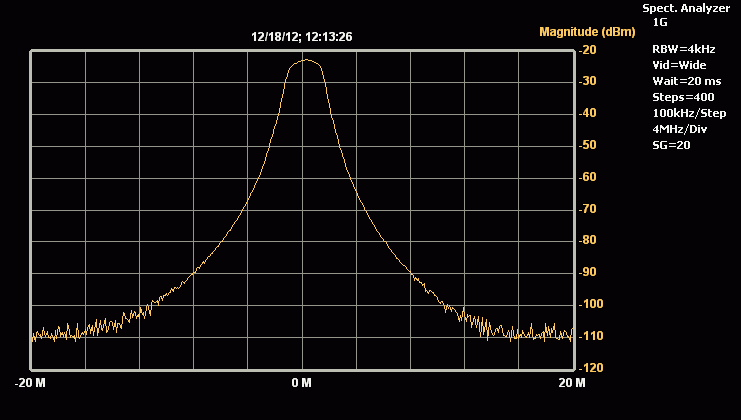
Example (Added 4-25-2019)
The following is a filter test using the procedure. The filter is the QMF 10725 from Hy-Q. It is well matched to 50 ohms.
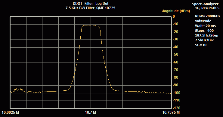
Path 5 is a direct path to the Log Detector. Even though the graph shows the RBW to be 2000 KHz, the actual bandwidth is dependent on the input to the Log Dectector, which is about 20 MHz. The Magnitude scale is calibrated for direct input to the Log Detector. Its dynamic range is from +10 dBm to -100 dBm.
Notice the spurious in the first division of the sweep. These are alias spurs created by the DDS. This is normal and Analog Devices specifies that any alias should be better than -70 dB below carrier (-70 dBc). These appear to be about -80 dBc so this is better than their specs. The top straight line trace is a direct short between the DDS 1 - J3 and the Log Detector. It is about -8 dBm. The peak magnitude of the filter is approximately -10.5 dBm. Therefore, the filter loss is about -2.5 dB. The filter's out-of-band response and input to output isolation is greater than -85 dBc. A very good filter.
I. Mixer 2 Module
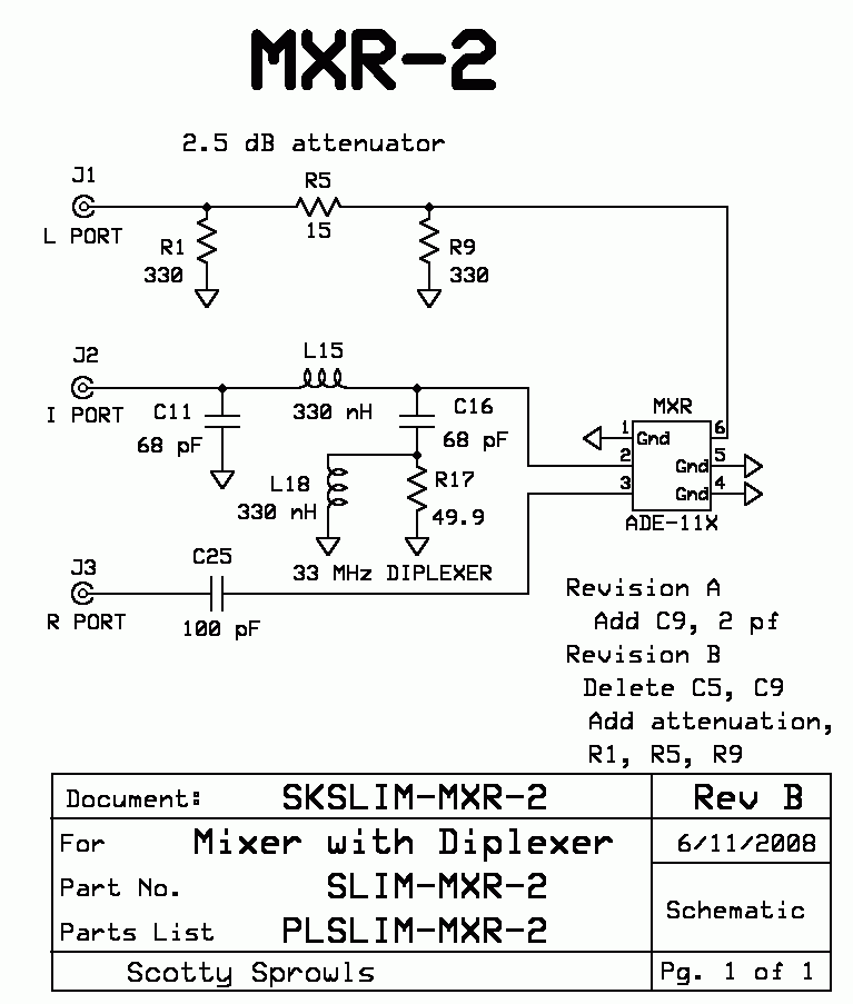
The Mixer 2 Module, SLIM-MXR-2, is the 2nd mixer within the spectrum analyzer circuit of the MSA. It should be tested and verified now so that it can be used in subsequent tests. The characteristics of the low pass filter (diplexer) in the I port path will be tested in a later test paragraph.
To test, the following items are required:
External DC power supply or wall wart rated at a nominal +13.6v, 1000 ma.
Computer, Monitor, and parallel printer port cable
Control Board
AtoD Module
Option, PDM Module
Log Detector Module
Master Oscillator
DDS 1 Module
Final Crystal Filter
Mixer 2 Module
DC Block
Software: spectrumanalyzer.tkn or spectrumanalyzer.bas
Set-up:

1. Verify the following SLIMs have their power and control wiring connected to the Control Board. Master Oscillator, DDS 1 Module, Log Detector, and AtoD Converter (and PDM module, if used).
2. Connect the J1 output of the Master Oscillator to the DC Block. Connect the DC Block to Mixer 2, J1. This connects to the internal 2.5 dB attenuator and then to the L port of the ADE-11X. The power level at the L port will be approximately +8.5 dBm., at 64 MHz. The DC Block is necessary since the J1 output of the Master Oscillator Module is DC coupled and the J1 input of Mixer 2 is at DC ground potential.
3. Connect the J2 output of the Master Oscillator to the J1 clock input of the DDS 1 Module.
4. Connect the J3 output of the DDS 1 Module to the Final Crystal Filter. The J3 output power will be approximately -8 dBm into the Final Crystal Filter.
5. Connect the Final Crystal Filter to the I port of the Mixer 2 Module, J2. The output power of the Filter, at its center frequency, will depend on the insertion loss of the Filter. The insertion loss was determined in the test paragraph, "Final Crystal Filter".
6. Connect the J3, R port output of the Mixer 2 Module to the Log Detector Module.
7. Connect the output of the Log Detector, J2, to the AtoD module, J1. Video Switch to "Mid".
8. Apply power to the Control Board. It supplies +10v power to the DDS Module, Master Oscillator, Log Detector, and AtoD module (or the PDM module).
Test
1. Run the MSA Program. The MSA Main Graph will open and sweep with the MSA in the Spectrum Analyzer mode.
2. If the Final Crystal Filter frequency is 10.7 MHz, the Magnitude trace may be displayed on the Graph. The level is not important yet.
3. Halt the Sweep. Open the Sweep Parameters Window. Change the Center Frequency (Cent) to the CF of your Final Crystal Filter. I will use the value, 10.7 MHz in this test. Change the Sweep Width (Span) to 10 times the bandwidth of your Final Crystal Filter. Click "OK". Click "Restart". Again, the Magnitude level is not important yet..
4. Halt the Sweep. Open the Special Tests Window by accessing the menu item, "Setup". Click the "DDS 1 Sweep" button. In the main Graph Window, click "Continue".
5. The resulting Magnitude trace should now indicate the bandwidth characteristics of your Final Crystal Filter. The maximum total power that is measured (Mag scale) is essentially the sum power of the two main products of the mixer, 53.3 MHz and 74.7 MHz. One half of this total power minus the input power to the mixer is the Conversion Loss of the mixer. Mixer Conversion Loss (and the Mixer Module) should be approximately -7 dB, +/- 1 dB. Example: If the output of the Final Crystal filter is -12 dBm, and the total power output of the mixer is -15.5 dBm, as indicated by the Magnitude scale (Log Det output), then the power of either signal is one half that, which is -18.5 dBm. The Conversion Loss is = -18.5 - (-12) = -6.5 dB. Any more than -8.5 dB of Conversion Loss would be considered a failure. Write down (on your Mixer 2 schematic) the Conversion Loss that you have calculated, for future reference.
Notice: These calculations are correct for the mixer action output, but does not take into consideration two important factors. First, the mixer port R has a 100 pfd capacitor in series with J3. This will cause a decrease in output power by a factor of about .4 dB. Second, the Log Detector will likely not have the same characteristics at 53.3 MHz and 74.7 MHz as it does at 10.7 MHz. Due to its input transformer bandwidth, the power measurement may be lower than expected by a factor of 1.6 dB. Therefore, the final mixer conversion loss may be in error by 2 dB.
6. The previous data will be fairly accurate if:
a. the Coarse Calibration of the Log Detector has been performed, and
b. the Magnitude of the signal outside of the Filter skirts is at least 15 dB below the power at the center frequency. This "outside" level is a portion of the 64 MHz LO signal that is passed from the L port of the ADE-11X mixer to its R port. This is mixer port isolation. At 10.7 MHz, the L to R port isolation should be at least -55 dB. Since the L port power is approximately +8 dBm, the "outside" power level should measure -47 dBm or lower.
c. The I to R port isolation should also be -55 dB or better. Therefore, the amount of 10.7 MHz input signal (-12 dBm) that will be passed to the output of the mixer will be less than -67 dBm.
7. This completes the main testing and verification for Mixer 2. I suggest you remove the Mixer 2 from your test set-up and substitute Mixer 1 in its place. Continue to the test paragraph, "Mixer 1 Module".
J. Mixer 1 Module
The Mixer 1 Module, SLIM-MXR-1, is the 1st mixer within the spectrum analyzer circuit of the MSA. It should be tested and verified now so that it can be used in subsequent tests. It can be tested the same way that Mixer 2 was previously tested and the results should be the same.

Set-Up and Test
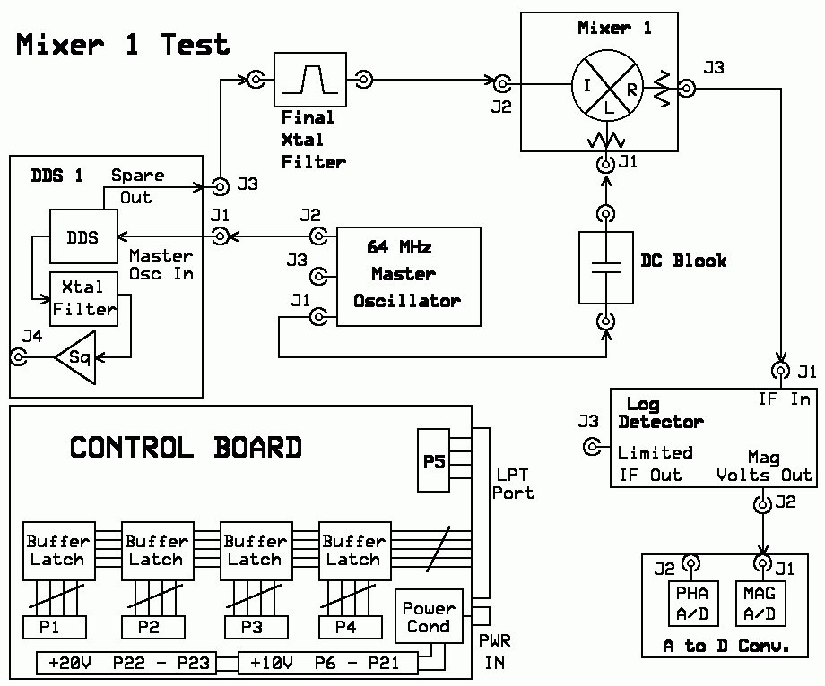
Use the procedure outlined in the paragraph, "Mixer 2 Module". Simply substitute the term Mixer 1 where the term "Mixer 2" is used.
If you have just completed the Mixer 2 testing, you may just remove Mixer 2 from the set-up and substitute the Mixer 1. If the sweep has been Halted, click "Continue". Return to test step 5. Write down the calculated insertion loss for Mixer 1 on your schematic.
After completing the Mixer 1 testing, I suggest you remove the Mixer 1 from your test set-up and substitute Mixer 3 in its place. Continue to the test paragraph, "Mixer 3 Module".
K. Mixer 3 Module
The Mixer 3 Module, SLIM-MXR-3, is the 3rd mixer within the MSA and is installed in the Tracking Generator circuit. It should be tested and verified now so that it can be used in subsequent tests. It can be tested the same way that Mixer 2 and Mixer 1 was previously tested but the results will differ, due to the attenuator circuit in the R port path.

Set-Up and Test

Use the procedure outlined in the paragraph, "Mixer 2 Module". Simply substitute the term Mixer 3 where the term "Mixer 2" is used. Halt your testing at the end of test step 4 (in the Mixer 2 paragraph) and continue below at step 5.
If you have just completed the Mixer 1 testing, you may just remove Mixer 1 from the set-up and substitute the Mixer 3. If the sweep has been Halted, click "Continue". Continue below at step 5.
5. The resulting Magnitude trace should now indicate the bandwidth characteristics of your Final Crystal Filter. The maximum total power that is measured (Mag scale) is essentially the sum power of the two main products of the mixer, 53.3 MHz and 74.7 MHz. One half of this total power minus the input power to the mixer is the Conversion Loss of the mixer module. Mixer Conversion Loss should be approximately -7 dB, +/- 1 dB. Module Conversion Loss should be approximately -21 dB, +/- 1 dB, due to the 14 dB attenuator in the R port circuit. Example: If the output of the Final Crystal filter is -12 dBm, and the total power output of the mixer module (J3) is -29.5 dBm, as indicated by the Magnitude scale (Log Det output), then the power of either signal is one half the total power, which would be -32.5 dBm. The Module's Conversion Loss is then = -32.5 - (-12) = -20.5 dB. Any more than -23 dB of Module Conversion Loss would be considered a failure. Write down (on your Mixer 3 schematic) the Conversion Loss that you have calculated, for future reference.
Notice: These calculations are correct for the mixer action output, but does not take into consideration an important factor. The Log Detector will likely not have the same characteristics at 53.3 MHz and 74.7 MHz as it does at 10.7 MHz. Due to its input transformer bandwidth, the power measurement may be lower than expected by a factor of 1.6 dB. Therefore, the final mixer conversion loss may be in error by 1.6 dB.
6. The previous data will be fairly accurate if:
a. the Coarse Calibration of the Log Detector has been performed, and
b. the Magnitude of the signal outside of the Filter skirts is at least 15 dB below the power at the center frequency. This "outside" level is a portion of the 64 MHz LO signal that is passed from the L port of the ADE-11X mixer to its R port. This is mixer port isolation. At 10.7 MHz, the L to R port isolation should be at least -55 dB. Since the L port power is approximately +8 dBm, the "outside" power level should measure -61 dBm or lower.
c. The I to R port isolation should also be -55 dB or better. Therefore, the amount of 10.7 MHz input signal (-12 dBm) that will be passed to the output of the mixer will be less than -81 dBm.
7. This completes the Mixer 3 testing. I suggest you remove the Mixer 3 from your test set-up and substitute Mixer 4 in its place. Continue to the test paragraph, "Mixer 4 Module".
L. Mixer 4 Module
The Mixer 4 Module, SLIM-MXR-4, is the 4th mixer within the MSA and is installed in the VNA phase detection circuit. It should be tested and verified now so that it can be used in subsequent tests. It can be tested the same way that Mixer 3 was previously tested and the results should be the same. The characteristics of the low pass filter (diplexer) in the I port path will be tested in a later test paragraph.

Set-Up and Test
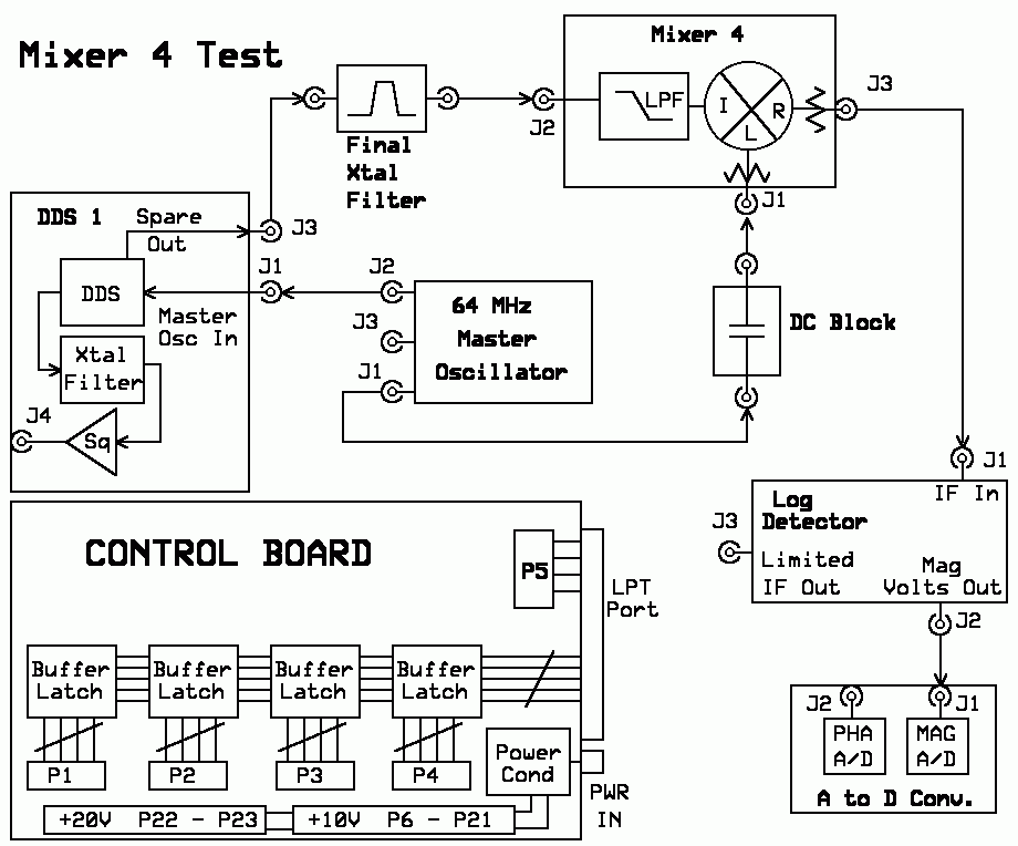
Use the procedure outlined in the paragraph, "Mixer 2 Module". Simply substitute the term Mixer 4 where the term "Mixer 2" is used. Halt your testing at the end of test step 4 (in the Mixer 2 paragraph) and continue below at step 5.
If you have just completed the Mixer 3 testing, you may just remove Mixer 3 from the set-up and substitute the Mixer 4. If the sweep has been Halted, click "Continue". Continue below at step 5.
5. The resulting Magnitude trace should now indicate the bandwidth characteristics of your Final Crystal Filter. The maximum total power that is measured (Mag scale) is essentially the sum power of the two main products of the mixer, 53.3 MHz and 74.7 MHz. One half of this total power minus the input power to the mixer is the Conversion Loss of the mixer module. Mixer Conversion Loss should be approximately -7 dB, +/- 1 dB. Module Conversion Loss should be approximately -21 dB, +/- 1 dB, due to the 14 dB attenuator in the R port circuit. Example: If the output of the Final Crystal filter is -12 dBm, and the total power output of the mixer module (J3) is -29.5 dBm, as indicated by the Magnitude scale (Log Det output), then the power of either signal is one half the total power, which would be -32.5 dBm. The Module's Conversion Loss is then = -32.5 - (-12) = -20.5 dB. Any more than -23 dB of Module Conversion Loss would be considered a failure. Write down (on your Mixer 4 schematic) the Conversion Loss that you have calculated, for future reference.
Notice: These calculations are correct for the mixer action output, but does not take into consideration an important factor. The Log Detector will likely not have the same characteristics at 53.3 MHz and 74.7 MHz as it does at 10.7 MHz. Due to its input transformer bandwidth, the power measurement may be lower than expected by a factor of 1.6 dB. Therefore, the final mixer conversion loss may be in error by 1.6 dB.
6. The previous data will be fairly accurate if:
a. the Coarse Calibration of the Log Detector has been performed, and
b. the Magnitude of the signal outside of the Filter skirts is at least 15 dB below the power at the center frequency. This "outside" level is a portion of the 64 MHz LO signal that is passed from the L port of the ADE-11X mixer to its R port. This is mixer port isolation. At 10.7 MHz, the L to R port isolation should be at least -55 dB. Since the L port power is approximately +8 dBm, the "outside" power level should measure -61 dBm or lower.
c. The I to R port isolation should also be -55 dB or better. Therefore, the amount of 10.7 MHz input signal (-12 dBm) that will be passed to the output of the mixer will be less than -81 dBm.
7. This completes the main testing and verification for Mixer 4. The characteristics of the low pass filter (diplexer) in the I port path will be tested in a later test paragraph.
M. PLO Module Tests
In the following paragraphs, the PLO Modules will be tested for basic operation. Voltage measurements are the only tests performed. This Test Diagram applies when testing any PLO.

N. PLO 2 Module
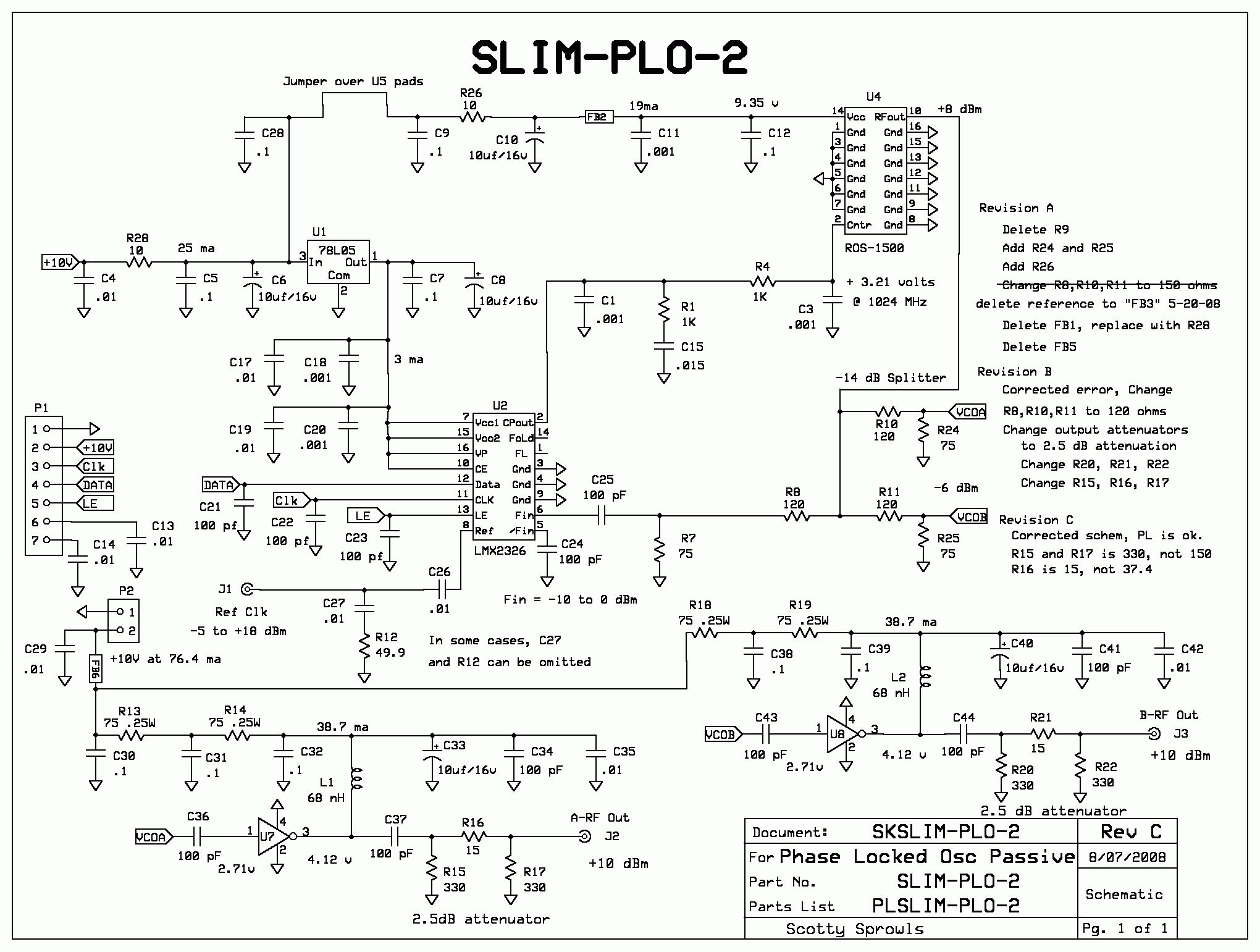
The PLO 2 Module, SLIM-PLO-2, is the fixed LO frequency source for the 2nd converter in the spectrum analyzer circuit of the MSA. It is also the fixed frequency source for the Tracking Generator circuit of the MSA. This paragraph will test the basic operation of the PLO 2. Subsequent test paragraphs will verify its output power and frequency stability.
This schematic is "scrunched" on the web page. Click on it to open in full view.
To test, the following items are required:
External DC power supply or wall wart rated at a nominal +13.6v, 1000 ma.
Computer, Monitor, and parallel printer port cable
Control Board
Master Oscillator
PLO 2 Module
Voltmeter
Software: spectrumanalyzer.tkn or spectrumanalyzer.bas
Set-up:
The following tests are also accurate if PLO 2 is tested in a completed and integrated MSA.
1. Verify the following SLIMs have their power and control wiring connected to the Control Board. Master Oscillator and PLO 2 Module.
2. Connect the output of the Master Oscillator J2 to J1 of the PLO 2 Module.
3. Apply power to the Control Board. It supplies +10v power to the Master Oscillator.
Test
1. Run the MSA Program. The MSA Main Graph will open and sweep with the MSA in the Spectrum Analyzer mode. PLO 2 will automatically be commanded to 1024 MHz. The Magnitude trace is meaningless. Halt the Sweep.
2. Measure and verify the voltage at these locations. Record them on your schematic.
a. P1-2 = +10 volts, +/- .2 volt.
b. U1-3 = +9.75 volts, +/- .2 volt.
c. Current = (voltage at a. - voltage at b.)/10 ohms = 25 ma., +/- 5 ma.
d. U2-7, U2-10, U2-15, U2-16 = +5.0 volts, +/-.1 volt
e. VCO supply voltage, U4-14 = +9.5 volts, +/-.2 volt (schematic voltage may not be correct)
f. VCO Current = (voltage at b. - voltage at e.)/10 ohms = 19 ma., +/- 5 ma.
g. FB6 / R13 = +10 volts, +/- .1 volt.
h. R14 / L1 = +4.12 volts, +/- .2 volt.
i. U7 Current = (voltage at g. - voltage at h.)/150 ohms = 39 ma., +/- 5 ma.
j. R19 / L2 = +4.12 volts, +/- .2 volt.
k. U8 Current = (voltage at g. - voltage at j.)/150 ohms = 39 ma., +/- 5 ma.
l. VCO Control Voltage, U4-2 = +3.2 volts, +/- .5 volt. If this voltage is +5 volts or 0 volts, it would indicate that PLO 2 is not locked.
3. The RF output power and frequency will be verified in subsequent test paragraphs.
O. PLO 1 Module
The PLO 1 Module, SLIM-PLO-1, is the variable frequency LO source for the 1st converter in the spectrum analyzer circuit of the MSA. It is also the variable frequency source for the VNA Phase circuit of the MSA. This paragraph will test the basic operation of the PLO 1. Subsequent test paragraphs will verify its output power and frequency stability.
This schematic is "scrunched" on the web page. Click on it to open in full view.

To test, the following items are required:
External DC power supply or wall wart rated at a nominal +13.6v, 1000 ma.
Computer, Monitor, and parallel printer port cable
Control Board
Master Oscillator
DDS 1 Module
PLO 1 Module
Voltmeter
Software: spectrumanalyzer.tkn or spectrumanalyzer.bas
Set-up:
The following tests are also accurate if PLO 1 is tested in a completed and integrated MSA.
1. Verify the following SLIMs have their power and control wiring connected to the Control Board. Master Oscillator, DDS 1 Module, and PLO 1 Module.
2. Connect the J1 output of the Master Oscillator to J1 of the DDS 1 Module.
2. Connect the J4 output of the DDS 1 Module to J1 of the PLO 1 Module.
3. Apply power to the Control Board. It supplies +10v power to the other SLIMs.
Test
1. Run the MSA Program. The MSA Main Graph will open and sweep with the MSA in the Spectrum Analyzer mode. PLO 1 will automatically be commanded to 1013.3 MHz, center frequency. The Magnitude trace is meaningless. Halt the Sweep.
2. Measure and verify the voltage at these locations. Record them on your schematic.
a. P1-2 / R28 = +10 volts, +/- .2 volt.
b. U1-3 and U5-3 = +9.70 volts, +/- .2 volt.
c. Current = (voltage at a. - voltage at b.)/10 ohms = 30 ma., +/- 5 ma.
d. U2-7, U2-10, U2-15, U2-16 = +5.0 volts, +/-.1 volt
e. U5-1 = +5.0 volts, +/-.1 volt
f. VCO supply voltage, U4-14 = +4.8 volts, +/-.1 volt
g. VCO Current = (voltage at e. - voltage at f.)/10 ohms = 19 ma., +/- 5 ma.
h. 20 volt supply, P1-6 / R27 = +19.0 volts, +/-.2 volt
i. U3 supply voltage, U3-7 = +18.94 volts, +/-.2 volt. If you have an optional oscilloscope, the peak to peak ripple at U3-7 should be less than 2 millivolts. The ripple frequency is between 8 KHz and 15 KHz.
j. U3 Current = (voltage at h. - voltage at i.)/24.9 ohms = 3 ma., +/- 1 ma.
k. Bias voltage, U3-3 = +2.5 volts, +/-.2 volt.
l. Loop Balance voltage, U3-2 = exactly the same as U3-3. Any error may indicate an unlocked condition. Your DVM must be high impedance (>1 Meg Ohms) for correct results.
m. VCO Control Voltage at U4-2 = +2.55 volts, +/- .5 volt. If this voltage is +19 volts or 0 volts, it would indicate that the PLL is definitely, not locked.
n. FB6 / R13 = +10 volts, +/- .1 volt.
o. R14 / L1 = +4.12 volts, +/- .2 volt.
p. U7 Current = (voltage at g. - voltage at h.)/150 ohms = 39 ma., +/- 5 ma.
q. R19 / L2 = +4.12 volts, +/- .2 volt.
r. U8 Current = (voltage at g. - voltage at j.)/150 ohms = 39 ma., +/- 5 ma.
3. The RF output power and frequency will be verified in subsequent test paragraphs.
P. PLO 3 Module
The PLO 3 Module is the variable frequency LO source for the converter in the Tracking Generator circuit of the MSA. It is also the variable frequency source for the VNA Phase circuit of the MSA. The PLO 3 Module is identical to the PLO 1 Module and share a common part number, SLIM-PLO-1. PLO 3 is tested the same way as PLO 1. The results are identical, with one exception. Since PLO 3 is commanded to 1034 MHz, the VCO Control Voltage will be different. This paragraph will test the basic operation of the PLO 3. Subsequent test paragraphs will verify its output power and frequency stability.
This schematic is "scrunched" on the web page. Click on it to open in full view. Note: The schematic is labeled SLIM-PLO-1 and is not an error. Both PLO 3 and PLO 1 use the same Module.
To test, the following items are required:
External DC power supply or wall wart rated at a nominal +13.6v, 1000 ma.
Computer, Monitor, and parallel printer port cable
Control Board
Master Oscillator
DDS 3 Module
PLO 3 Module
Voltmeter
Software: spectrumanalyzer.tkn or spectrumanalyzer.bas
Set-up:
The following tests are also accurate if PLO 3 is tested in a completed and integrated MSA.
1. Verify the following SLIMs have their power and control wiring connected to the Control Board. Master Oscillator, DDS 3 Module, and PLO 3 Module.
2. Connect the J3 output of the Master Oscillator to J1 of the DDS 3 Module.
2. Connect the J4 output of the DDS 3 Module to J1 of the PLO 3 Module.
3. Apply power to the Control Board. It supplies +10v power to the other SLIMs.
Test
1. Run the MSA Program. The MSA Main Graph will open and sweep with the MSA in the Spectrum Analyzer mode. PLO 3 will automatically be commanded to a fixed frequency of 1034 MHz. The Magnitude trace is meaningless. Halt the Sweep.
2. Measure and verify the voltage at these locations. Record them on your schematic.
a. P1-2 / R28 = +10 volts, +/- .2 volt.
b. U1-3 and U5-3 = +9.70 volts, +/- .2 volt.
c. Current = (voltage at a. - voltage at b.)/10 ohms = 30 ma., +/- 5 ma.
d. U2-7, U2-10, U2-15, U2-16 = +5.0 volts, +/-.1 volt
e. U5-1 = +5.0 volts, +/-.1 volt
f. VCO supply voltage, U4-14 = +4.8 volts, +/-.1 volt
g. VCO Current = (voltage at e. - voltage at f.)/10 ohms = 19 ma., +/- 5 ma.
h. 20 volt supply, P1-6 / R27 = +19.0 volts, +/-.2 volt
i. U3 supply voltage, U3-7 = +18.94 volts, +/-.2 volt. If you have an optional oscilloscope, the peak to peak ripple at U3-7 should be less than 2 millivolts. The ripple frequency is between 8 KHz and 15 KHz.
j. U3 Current = (voltage at h. - voltage at i.)/24.9 ohms = 3 ma., +/- 1 ma.
k. Bias voltage, U3-3 = +2.5 volts, +/-.2 volt.
l. Loop Balance voltage, U3-2 = exactly the same as U3-3. Any error may indicate an unlocked condition. Your DVM must be high impedance (>1 Meg Ohms) for correct results.
m. VCO Control Voltage at U4-2 = +2.90 volts, +/- .5 volt. If this voltage is +19 volts or 0 volts, it would indicate that the PLL is definitely, not locked. Notice the voltage is about .17 volts higher than what was measured during the PLO 1 test. This is due to the difference in frequencies.
n. FB6 / R13 = +10 volts, +/- .1 volt.
o. R14 / L1 = +4.12 volts, +/- .2 volt.
p. U7 Current = (voltage at g. - voltage at h.)/150 ohms = 39 ma., +/- 5 ma.
q. R19 / L2 = +4.12 volts, +/- .2 volt.
r. U8 Current = (voltage at g. - voltage at j.)/150 ohms = 39 ma., +/- 5 ma.
3. The RF output power and frequency will be verified in subsequent test paragraphs.
Q. PLO Frequency and RF Power test.
The previous testing of PLO 1, PLO 2, and PLO 3 verified basic operation only. This paragraph will verify frequency and the power level of each PLO output.
To test, the following items are required:
External DC power supply or wall wart rated at a nominal +13.6v, 1000 ma.
Computer, Monitor, and parallel printer port cable
Control Board
Log Detector Module
A to D Converter Module
PDM Module (VNA option)
Master Oscillator
PLO 2 Module
DDS 1 Module
PLO 1 Module
DDS 3 Module (Tracking Generator option)
PLO 3 Module (Tracking Generator option)
Mixer 2 Module
Final Crystal Filter
Coaxial Attenuator, 10 dB to 20 dB
Software: spectrumanalyzer.tkn or spectrumanalyzer.bas
Set-up:
1. Verify the following SLIMs have their power and control wiring connected to the Control Board. Log Detector Module, A to D Converter Module, PDM Module (VNA option), Master Oscillator, PLO 2 Module, DDS 1 Module, and PLO 1 Module. Connect DDS 3 Module, and PLO 3 Module if used in MSA.
2. Connect the J1 output of the Master Oscillator to J1 of the DDS 1 Module.
3. Connect the J2 output of the Master Oscillator to J1 of the PLO 2 Module.
4. Connect the J3 output of the Master Oscillator to J1 of the DDS 3 Module.
5. Connect the J4 output of the DDS 1 Module to J1 of the PLO 1 Module.
6. Connect the J4 output of the DDS 3 Module to J1 of the PLO 3 Module.
7. Connect the J2 output of the Log Detector Module to J1 of the AtoD Module. Video Switch to "Mid".
8. Connect the output of the Final Crystal Filter to J1 of the Log Detector Module.
9. Connect the J2 output of the Mixer 2 Module to the Final Crystal Filter.
10. Connect the J2 output of the PLO 2 Module to J1 of the Mixer 2 Module.
11. Connect the J2 output of the PLO 1 Module to the Coaxial Attenuator.
12. Connect the output of the Coaxial Attenuator to J3 of the Mixer 2 Module.
13. Apply power to the Control Board. It supplies +10v power to the other SLIMs.

Test
1. Run the MSA Program. The MSA Main Graph will open and sweep with the MSA in the Spectrum Analyzer mode.
2. The Magnitude response will be a representation of the Final Crystal Filter characteristics. The center of the filter response should be very close to the center of the graph. Don't be concerned if it is not, since the Frequency Calibration of the Master Oscillator has not been performed. We are concerned with only two results in this test, Magnitude power and frequency stability.
3. The 3 dB bandwidth of the response should be the expected 3 dB bandwidth of the Final Crystal Filter. This verifies that both PLO 1 and PLO 2 are locked to the correct frequencies. If it is wider, it may indicate that either PLO 1 or PLO 2 is not fully locked.
4. The Magnitude at the center of the response will be used to calculate the RF output level at J2 of PLO 1. I will use the value, -13 dBm as a Magnitude measurement example. We will use the following information to determine the PLO output level.
a. We have tested the Final Crystal Filter to obtain its Insertion Loss. (IL)(I will use 4 dB)
b. We have tested the Mixer 2 to obtain its Conversion Loss. (CL)(I will use 6.5 dB)
c. We have coarsely calibrated the Log Detector Module to indicate a fairly accurate input power level.
d. The power of the PLO 1 can be calculated by: P = Magnitude measurement + IL + CL + Attenuator.
Example: P = -13 dBm + 4 dB + 6.5 dB +10 dB = +7.5 dBm.
e. Calculate the Power output of your PLO 1, J2 and write the result on the PLO 1 schematic. Expect a power output of +9 dBm, +/- 2 dB. (I expect to hear a variety of results from builders. So far, many have reported low output power from PLO 1 and PLO 3 (in the range of +7 dBm, +/- 1 dB).
5. Reconfigure to measure the power output of PLO 1 - J3.

a. Connect the J3 output of the PLO 1 Module to the Coaxial Attenuator.
b. Calculate the Power output of PLO 1, J3 using the same calculation and write the result on the PLO 1 schematic. Expect a power output of +9 dBm, +/- 2 dB.
6. Reconfigure to measure the power output of PLO 2 - J2.

a. Connect the J2 output of the PLO 2 Module to the Coaxial Attenuator.
b. Connect the J2 output of the PLO 1 Module to J1 of the Mixer 2 Module.
c. Calculate the Power output of PLO 2, J2 using the same calculation and write the result on the PLO 2 schematic. Expect a power output of +9 dBm, +/- 2 dB.
7. Reconfigure to measure the power output of PLO 2 - J3.
a. Connect the J3 output of the PLO 2 Module to the Coaxial Attenuator.
b. Connect the J2 output of the PLO 1 Module to J1 of the Mixer 2 Module.
c. Calculate the Power output of PLO 2, J3 using the same calculation and write the result on the PLO 2 schematic. Expect a power output of +9 dBm, +/- 2 dB.
The following will test PLO 3 if it used in the MSA.
8. Reconfigure to measure the power output of PLO 3 - J2.

a. Connect the J2 output of the PLO 3 Module to the Coaxial Attenuator.
b. Connect the J2 output of the PLO 2 Module to J1 of the Mixer 2 Module.
c. If sweeping in the SA Mode, halt the sweep.
d. Change Mode to SA with Tracking Generator.
e. Halt the sweep.
f. Open Sweep Parameters Window and change the Center Frequency to center frequency of the Final Crystal Filter (ie. 10.7). Click the "OK" button to close the window.
g. Click "Restart". This will command the PLO 3 to sweep, centered at 1034.7 MHz.
h. Calculate the Power output of PLO 3, J2 using the same calculation and write the result on the PLO 3 schematic. Expect a power output of +9 dBm, +/- 2 dB.
9. Reconfigure to measure the power output of PLO 3 - J3.

a. Connect the J3 output of the PLO 3 Module to the Coaxial Attenuator.
b. Connect the J2 output of the PLO 2 Module to J1 of the Mixer 2 Module.
c. Calculate the Power output of PLO 3, J3 using the same calculation and write the result on the PLO 3 schematic. Expect a power output of +9 dBm, +/- 2 dB.
R. Phase Detector Module
The main purpose of this paragraph is to test the operation of the Phase Detector Module, SLIM-PDM. It is also used to test the operation and Frequency Range of the Tracking Generator/VNA. This paragraph is used only for the MSA with the Tracking Generator option or VNA extension. Basic MSA (Spectrum Analyzer only) users may skip this paragraph.

To test, the following items are required:
External DC power supply or wall wart rated at a nominal +13.6v, 1000 ma.
Computer, Monitor, and parallel printer port cable
Volt-Ohm Meter (VOM, Digital or Analog). All voltage measurements are DC unless noted.
Control Board
Log Detector Module
A to D Converter Module
PDM Module (VNA option)
Master Oscillator
DDS 1 Module
PLO 1 Module
DDS 3 Module (Tracking Generator option)
PLO 3 Module (Tracking Generator option)
Mixer 2 Module
Mixer 4 Module (VNA option)
Final Crystal Filter
Coaxial Attenuator, 10 dB to 20 dB
Software: spectrumanalyzer.tkn or spectrumanalyzer.bas
Set-up:
1. Verify the following SLIMs have their power and control wiring connected to the Control Board. Log Detector Module, A to D Converter Module, PDM Module (VNA option), Master Oscillator, DDS 3 Module, PLO 3 Module, DDS 1 Module, and PLO 1 Module.
2. Connect the J1 output of the Master Oscillator to J1 of the DDS 1 Module.
3. Connect the J3 output of the Master Oscillator to J1 of the DDS 3 Module.
4. Connect the J4 output of the DDS 1 Module to J1 of the PLO 1 Module.
5. Connect the J4 output of the DDS 3 Module to J1 of the PLO 3 Module.
6. Connect the J2 output of the Log Detector Module to J1 of the AtoD Module. Video Switch to "Mid".
7. Connect the output of the Final Crystal Filter to J1 of the Log Detector Module.
8. Connect the J2 output of the Mixer 2 Module to the Final Crystal Filter.
9. Connect the J2 output of the PLO 3 Module to J1 of the Mixer 2 Module.
10. Connect the J3 output of the PLO 3 Module to J3 of the Mixer 4 Module.
11. Connect the J2 output of the PLO 3 Module to J1 of the Mixer 4 Module.
12. Connect the J2 output of the Mixer 4 Module to J1 of the Phase Detector Module. (VNA option)
13. Connect the J3 output of the Log Det Module to J2 of the Phase Detector Module. (VNA option)
14. Connect the J3 output of the Phase Detector Module to J2 of the AtoD Module. (VNA option)
15. Connect the J3 output of the PLO 1 Module to the Coaxial Attenuator.
16. Connect the output of the Coaxial Attenuator to J3 of the Mixer 2 Module.
17. Apply power to the Control Board. It supplies +10v power to the other SLIMs.
Test
1. Run the MSA Program. The MSA Main Graph will open and sweep with the MSA in the Spectrum Analyzer mode. The trace results are meaningless.
2. Halt the Sweep
3. If the PDM is installed, change Mode to VNA-Transmission Mode. If the PDM is not installed, change Mode to SA with Tracking Generator Mode.
4. Halt the Sweep
5. Open the Sweep Parameters Window and change:
a. Center Frequency to 600 (MHz)
b. Span to 1200 (MHz)
c. Wait to 50
6. Click "OK" to close Sweep Parameters Window.
7. Click "Restart".
8. The Magnitude trace should be about -11 dBm, +/- 2 dB from 0 MHz to at least 1000 MHz. Above that, the Magnitude trace will fall off where either PLO 1 or PLO 3 reaches its frequency limit. The Phase trace may be at any value (in degrees). The amount of Phase shift vs. frequency depends on the length of the test cables. If all are exactly the same length, you will not see a phase change vs. frequency.
Note: The following voltage measurements are valid only when the PDM has both its input signals present, that is, when in the VNA Mode (either Transmission or Reflection).
9. Measure and verify the voltage at these locations. Record them on your schematic.
a. P1-2 / R11 = +10 volts, +/- .1 volt.
b. U1-3 = +9.50 volts, +/- .1 volt.
c. Current = (voltage at a. - voltage at b.)/10 ohms = 50 ma., +/- 5 ma.
d. U5-2, U5-7, U5-8, U2-5, U6-5 = +5.0 volts, +/-.1 volt
e. U3-5, U7-5 = 25 mv less that measured at step d, +/- 5 mv.
f. U4-5 = 15 mv less that measured at step d, +/- 2 mv.
g. U9-2, U9-7, U9-8 = 18 mv less that measured at step d, +/- 2 mv.
h. U8-2, U8-7, U8-8 = 18 mv less that measured at step d, +/- 2 mv.
i. U2-1, U6-1 = +2.50 volts, +/- .1 volt.
10. If you have an optional oscilloscope with at least a 20 MHz bandwidth, measure:
a. J1 = 200 mv peak to peak, +/- 50 mv
b. J2 = 40 mv peak to peak, +/- 10 mv
This completes the PDM test, but you may wish to keep all the modules in place to test the Coaxial Cavity Filter.
S. Coaxial Cavity Filter
Updated Feb. 10, 2014
The Coaxial Cavity Filter is best tuned when it is integrated into its proper location within the MSA. This is between Mixer 1 and Mixer 2. That procedure is performed after the MSA is fully integrated and can be found on the page, Testing the Integrated MSA, "Coaxial Cavity Filter Test".
However, the filter can be functionally tested before final MSA integration. The following test procedure will verify the functionality of the filter and will allow for coarse tuning. The test procedure is valid for all MSA options: Basic MSA, MSA/TG, or MSA/TG/VNA. It is important that these preliminary steps are taken before this test is performed.
1. The Master Oscillator Frequency must be determined and its value entered into the Configuration Manager of the MSA Program.
2. The Final Crystal Filter center frequency must be determined and its value entered into the Configuration Manager of the MSA Program.
3. Coarse Calibration of Log Detector must have been performed. See Step G on this page.
Coaxial Cavity Filter Test for Basic MSA
Configure your MSA into its final topology with the following exceptions:
1. Leave out the Mixer 1 and the I.F. Amplifier Module. They are not required for this test.
2. Connect the J2 output of the Mixer 2 Module to J1 of the Log Detector Module.
3. Connect the J3 output of the PLO 1 Module to J1 a 10 dB to 20 dB Attenuator.
4. Connect the output of the Attenuator to the J3 input of Mixer 2.
5. AtoD Module Video Switch to "Mid".
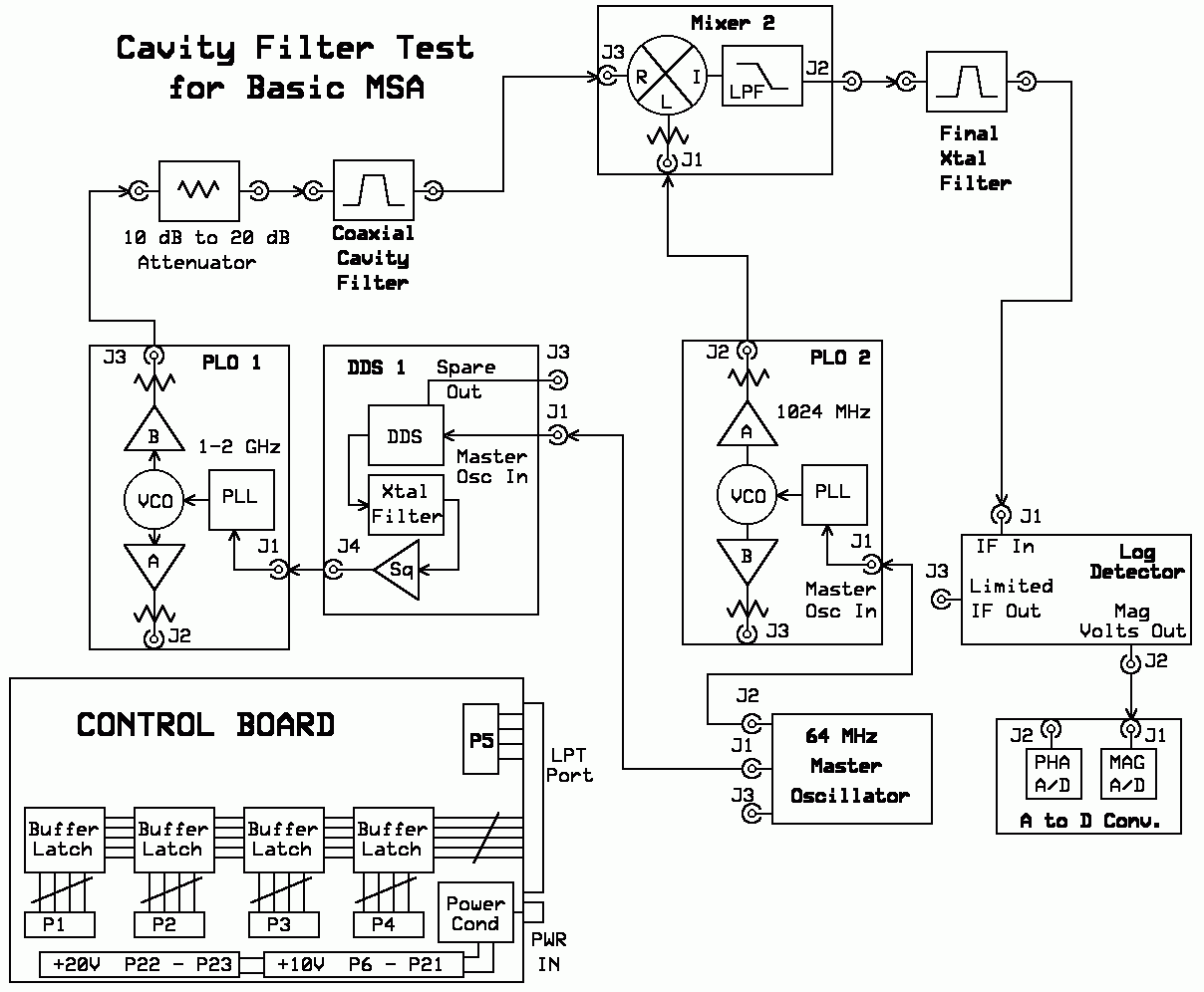
Test
1. Run the MSA Program. The MSA Main Graph will open and sweep with the MSA in the Spectrum Analyzer mode.
2. Halt the Sweep and open the Sweep Parameters Window and change:
a. Center Frequency to 0 (MHz).
b. Span to 40 (MHz).
c. Steps to 400
d. Wait to 20
3. Click "OK" to close Sweep Parameters Window.
4. Click "Restart"; then click "Halt"
5. Open Special Tests Window (under menu item "Setup")
6. Click "Cavity Filt Test" button. Leave Special Tests Window open. Close only after test is complete.
7. The Cavity Filter is swept by the frequency of PLO1 (the feed-thru of Mixer1 L to R port isolation). PLO1 is stepped in 100 KHz increments and PLO 2 will follow PLO1 at a frequency 10.7 MHz higher than PLO1. The Log Detector responds to this difference in frequency (10.7 MHz).
8. The Magnitude trace will show the bandwidth response of the Cavity Filter. The frequencies displayed are offset below the actual frequencies of the Cavity Filter. That is, the center of 0M corresponds to 1013.3 MHz, the -20M corresponds to 993.3 MHz, and 20M is 1033.3 MHz. The Magnitude is totally dependent on the Isolation of Mixer 1 (L to R ports). The Magnitude should be approximately -22 dBm plus or minus a few dB.
9. Tune your Coaxial Cavity Filter for best response, with its center at "0" MHz.
*Note: There might be a discontinuity in the center (0 Hz). Don't worry about it. This is an interference problem with this test, but does not affect the completed MSA.
10. The insertion loss of the Cavity Filter should be approximately -6 dB, +/- 2 dB. You can determine this by replacing the Cavity Filter with a short coax cable and note the different Magnitude level of the sweep.
11. The peak Magnitude power at "0" MHz will depend on component losses. The total power read at the Log Detector is = (LO 1 output Power) - (Attenuator) - (Mixer 2 Insertion Loss) - (Cavity Filter Loss) - (Final Crystal Filter Loss).
Example: Log Det pwr = +9 dBm - 10 dB - 6.5 dB - (6 dB) - (4 dB) = -17.5 dBm.
T. IF Amplifier Module
Updated Feb. 10, 2014 Modify Coaxial Cavity Filter Test to use the "Special Tests" Window.
Updated July 3, 2015 Add comments to Mixer Tests
Updated Sept 9, 2016 Section H, Filter Test procedure.
Updated Feb 23, 2018
You can link to a SLIM's web page by clicking on the module's test paragraph header. Here are other links supporting the MSA :
Main Page for MSA Main page for the MSA.
Construction page for the SLIM MSA.
Testing the Integrated MSA. The test procedure to use if your MSA is fully integrated, and you wish to test it without disconnecting cables, or if your completed MSA uses the direct coaxial connection scheme.
The purpose of this page is to help the MSA builder test his SLIM modules as he completes and integrates them into the MSA system. These test procedures assume the MSA is using SLIMs with RF connectors (the MSA is not using the direct coaxial connection scheme). This page is not intended to fully test any single SLIM (stand-alone). This would require test equipment that many builders do not have.
Thefore, multiple test paragraphs will verify the operation of each SLIM, although you may find that a SLIM is not fully verified by the end of its test paragraph. This is because many of the SLIM modules require other supporting SLIM modules to have been completed and integrated before its full functionality is verified. However, by following the build and test chronology, each SLIM will have been fully verified by the end of this page.
The set-ups and procedures will be explained the first time they are presented, and then only referenced in later paragraphs. This page can also be used as a guide for integration testing using modules that were constructed before the SLIM designs.
I would like to add a comment for those who wish to test the SLIMs as they build them. Be very, VERY careful when probing around in an active SLIM. In my many years of experience, I have destroyed many circuits by "a slip of a probe". I'd like to repeat this several times, but I'm sure you get the message.
MSA Build Chronology
For MSA integration and verification, the SLIMs should be constructed in this order:
Control Board, SLIM-CB-NV
Phase Detector Module, SLIM-PDM. (for VNA extension)
A to D Converter Module, SLIM-ADC-16 or SLIM-ADC-12
Log Detector Module, SLIM-LD-8306
Master Oscillator Module, SLIM-MO-64
DDS 1 Module, SLIM-DDS-107 (and DDS 3 Module for MSA/TG)
Final Crystal Filter (Resolution Filters)
Mixer 2, SLIM-MXR-2
Mixer 1, SLIM-MXR-1
Mixer 3, SLIM-MXR-3 (for Tracking Generator addition)
Mixer 4, SLIM-MXR-4 (for VNA extention)
PLO 2, SLIM-PLO-2
PLO 1, SLIM-PLO-1 (and PLO 3 for Tracking Generator addition)
Coaxial Cavity Filter
I.F. Amplifier Module, SLIM-IFA-33
Testing the SLIMs for the MSA
The following Test Paragraphs should be accomplished in this order:
A. Control Board
B. A to D Converter Module
C. Log Detector Module
D. Master Oscillator Module
E. DDS 1 Module
F. DDS 3 Module for MSA/TG
G. Coarse Calibration of Log Detector
H. Final Crystal Filter (Resolution Filters).
I. Mixer 2 Module
J. Mixer 1 Module
K. Mixer 3 Module, (for MSA/TG)
L. Mixer 4 Module, (for MSA/VNA)
M. PLO Module Tests
N. PLO 2 Module
O. PLO 1 Module
P. PLO 3 Module, (for MSA/TG)
Q. PLO Frequency and RF Power test
R. Phase Detector Module
S. Coaxial Cavity Filter
T. I.F. Amplifier Module
Test Equipment and Other Items Required for Integration Testing:
External DC power supply or wall wart rated at a nominal +13.6v, 1000 ma.
Volt-Ohm Meter (VOM, Digital or Analog). All voltage measurements are DC unless noted.
Optional Oscilloscope (1 MHz BW or better), but may be manditory for troubleshooting a faulty module.
DC Block (a .1 ufd mounted in series between two RF connectors)
Computer with LPT port, monitor, and parallel printer port cable (or optional USB Control)
Software: It is assumed that the latest MSA Software has been downloaded from the MSA Web Site and has been initialized. If you are not sure your's is the latest, go to the Web Page: MSA Set Up and Calibration. Follow the instructions for inital running of the MSA Software. Later references to this process will state: "Run the MSA Program", which is "spectrumanalyzer.bas" application with Liberty Basic as the main program, or "spectrumanalyzer.exe" application without Liberty Basic.
Block Diagram for the MSA/VNA
Wiring Diagram for the MSA/VNA
Testing the SLIM's for the MSA
A. Control Board
The Control Board contains all of the interfacing between the computer and the individual modules. It also contains the voltage regulation needed for the other modules. The Control Board requires +12 to +15 volts DC and 30 ma of current. appx. For full MSA operation, the Control Board will use and pass on about 750 ma.
To test, the following items are required:
External DC power supply or wall wart rated at a nominal +13.6v, 1000 ma.
Computer, Monitor, and parallel printer port cable
DC voltmeter
Oscilloscope (1 MHz BW or better) is optional
Control Board
MSA Software: Version 116 or later
Test Procedure:
1. Apply power (+13.6 v nominal) to the Control Board.
2. Connect the Control Board LPT connector to the Parallel Port of the Computer.
This is the latest schematic of the MSA Control Board. If your Control Board is an earlier version, you will want to test if pull-up resistors are required for your computer. Most home computers do not need them.
3. Measure the voltage at these locations, as indicated in the schematic:
SELECT, PE, WAIT, and ACK. The voltage should read a minimum of 2.0 volts, maximum of 5.0 volts. If you read less than the minimum voltage, remove power, disconnect from the computer and add the pull-up resistors, R9-R12.
Basic Voltage Tests:
1. Measure the input voltage to the Control Board at U5-1. Range: +12.0 v to +18 v.
2. Measure the output of the +10 volt regulator, U5-3. It should be +10.0 volts, +/- 0.2 volts.
3. Measure the output of the +5 volt regulator, U6-1. It should be +5.0 volts, +/- 0.2 volts.
4. LED 1 should be lit.
5. Measure the output of the +20 volt multiplier at P23-2 and P24-2. It should be +19.3 volts, +/- 0.3 volts. This is an unloaded voltage test since PLO 1 and PLO 3 are not connected to the Control Board. When they are, this voltage will drop to +18.94 volts +/- .3 volts.
6. If you have an oscilloscope, measure the peak to peak ripple at P23-2 or P24-2. It should be less than 5.0 millivolts. When loaded by PLO 1 and PLO 3, this peak to peak ripple should be less than 20.0 millivolts. When the MSA is completed, excessive ripple will be seen as side bands on every signal when in the Spectrum Analyzer Mode. A cure is too add more capacitance at C20, C21, C23, C24, and C25.
7. If C15 is installed, measure the -10 volt multiplier at P23-3 and P24-3. It should be -10.0 volts, +/- 0.3 volts. The -10 volts is not used in the SLIM MSA, but can be utilized for external experiments requiring current less than 20 ma.
Testing the LPT Port (the Control Board is not required for this test)
1. Run the MSA Program. Halt and open Special Tests Window under the Menu item, "Setup". The "Special Tests Window" will open. Click the "LPT Port Test" button. The LPT Printer Port Test window will open.
2. Any port line can be set to either a "0" or a "1" by clicking the appropriate Button. The LPT port pin numbers are shown for each bit.
3. Click the "CAPTURE STATUS" button. If the LPT port is disconnected, AND the computer's LPT port does not require pull-ups, all bits should register "1".
Testing the Control Board Outputs
1. Connect the Computer's LPT port to the Control Board's LPT connector.
2. Run the MSA Program. Halt and open Special Tests Window under the Menu item, "Setup". The "Special Tests Window" will open. Click the "LPT Port Test" button. The LPT Printer Port Test window will open.
3. You are able to change each Control Board output bit independently by Enabling the appropriate buffer and then clicking on the respective LPT Pin box. Use the following table. You can use the DC voltmeter or oscilloscope for verification.
Buffer Enable Control Output
U1 Pin 17, Sel = 1 P1 pins 2-9
U2 Pin 16, Init = 1 P2 pins 2-9
U3 Pin 14, Auto = 1 P3 pins 2-9
U4 Pin 1, Strobe = 1 P4 pins 2-9
Testing the Control Board Inputs (Status Bits)
The 5 Status Pins will be read when the "CAPTURE STATUS" button is pressed. The Status Pins are LPT-pin 11 for WAIT, LPT-pin 10 for ACK, LPT-pin 12 for PE, and LPT-pin 13 for Select. LPT-pin 15 is ERROR. Although ERROR is not connected to anything on the Control Board, it can be toggled by shorting LPT pin 15 to ground.
1. Click the "CAPTURE STATUS" button. All status bits should read "1". You can then short any of the 5 status pins to ground and the bit status (when clicked) will read (0) on the pin that was grounded.
If these controls do not work, it indicates that your computer LPT 1 is either:
a. not set up for the correct COM port within the computer. or
b. the LPT Port Address is not correct
B. AtoD Module
The following test procedure is written for the SLIM-ADC-16. The procedure is the same when using the SLIM-ADC-12.
To test, the following items are required:
External DC power supply or wall wart rated at a nominal +13.6v, 1000 ma.
Computer, Monitor, and parallel printer port cable
DC voltmeter
Oscilloscope (1 MHz BW or better) is optional
Control Board
AtoD Module (and PDM Module if AtoD requires its power)
Software: MSA Program in: spectrumanalyzer.tkn or spectrumanalyzer.bas
If the SLIM-ADC-16 has been constructed for use in the Basic MSA only, the U1 voltage regulator will be installed. If constructed for the MSA/VNA, U1 may be omitted. If so, the SLIM-PDM module must be integrated into the system so that its 5 volt power can supply the AtoD module. Make sure the PDM module has its ferrite jumpers installed (FBx and FB2).
This schematic shows the U1 regulator installed. If it is not there must be a jumper wire from the pwb pads of U1-3 to U1-1. Power is supplied from the PDM module's J2-1 and J2-2 to the AtoD module's J1-1 and J1-2. The name "+10v" should be changed to "+5v".
Test Procedure:
Set Up: Connect AtoD module's harness wiring to Control Board and PDM module if used. The J1 and J2 inputs of the AtoD should not connected to anything for the following test. The Video Selection switches must be connected.
1. Apply power to the Control Board. It supplies +10v power to the AtoD module or the PDM module.
Verify the voltage at U1-3 is +10 volts, +/- .2 volts.
2. Measure the +5 volts at U1-1, U2-1, U2-2, U2-9, U2-10. It should be +5.0 volts, +/- .1 volts.
3. Measure the +5 volts at U3-1, U3-2, U3-9, U3-10. It should be +5.0 volts, +/- .1 volts. U3 does not need to be installed for the Basic MSA version.
4. Measure the voltage at U2-3 (and U3-3 if installed). With a high impedance VOM, this point will read somewhere around 30 millivolts. A 0 volts reading might indicate a short or low resistance path to ground. A much higher voltage might indicate a short or low resistance path to +5v. If so, inspect for shorts or cleanliness. It will probably read 0 volts with an analog VOM.
5. Run the MSA Program. The MSA Main Graph will open and sweep with the MSA in the Spectrum Analyzer mode. The Magnitude trace will probably be a straight horizontal line at the bottom of the graph. This is because the voltage level at the AtoD J1 is close to 0 volts. Select the Video Switch to "Mid", to add video filtering capacitance to the J1/J2 input circuits.
Magnitude AtoD test
1. Use your voltmeter as a resistance path to increase the voltage at J1. Place the negative probe on the circuit trace of the Magnitude input of the AtoD module, J1. Place the positive probe on a circuit trace that is +5 volts. The Magnitude trace should shift from the bottom of the graph to the top of the graph. The voltmeter will read 0 volts when the circuit has charged the video capacitor to +5 volts and the circuit is stable.
2. Remove the probes and the Magnitude trace will eventually seek the lowest Magnitude level on the graph. This is due to the decay of the video capacitor.
3. In each of these steps, you may look at the AtoD bit value that is created for Magnitude. Halt the sweep and open the Variables Window. Click "Continue". The Magdata bit value will update during the sweep.
4. If the Log Detector module is connected to the AtoD converter, it should be powered up. In this case, the Magnitude trace may not be at the lowest level. The voltmeter probe test will not work.
Phase AtoD test
1. Halt the sweep. Change the MSA mode to VNA-Transmission Mode
2. The MSA will begin sweeping and the Phase trace will indicate what looks like multiple vertical line patterns. This is because the voltage level at the AtoD J2 is close to 0 volts.
3. Halt the sweep. Open the Special Tests Window. Click the "Change PDM" button until it reads "PDM in Normal".
4. Click "Continue". The Phase trace will become a straight horizontal line in the center of the graph, indicating 0 degrees.
5. Halt the sweep. Click the "PDM in Normal" button until it reads "PDM in Inverted".
6. Click "Continue". The Phase trace will become a straight horizontal line at the bottom of the graph, indicating =180 degrees.
7. Use your voltmeter as a resistance path to increase the voltage at J2. Place the negative probe on the circuit trace of the Phase input of the AtoD module, J2. Place the positive probe on a circuit trace that is +5 volts. The Phase trace should shift from the bottom of the graph to the top of the graph. The voltmeter will read 0 volts when the circuit has charged the video capacitor to +5 volts and the circuit is stable.
8. If the PDM module is powered up and connected to the AtoD converter, the connections (PDM-J3 to ADC-J2) must be removed to allow these tests to work.
C. Log Detector Module
The Log Detector Module, SLIM-LD-8306, converts RF power to voltage in a logarithmic function. The bandwidth of the module is 2 MHz to 160 MHz, although the input will be 10.7 MHz in the MSA.
The J2 output is the Magnitude voltage output which goes to the AtoD Module. Its J1 input dynamic range is from approximately -90 dBm to +10 dBm, although this range might be extended. Its J2 output voltage over this range is approximately .35 volts to 2.35 volts.
The J3 output is an RF Limited output of the input frequency. It supplies the Signal Input to the PDM Module (VNA only). The module does not require any direct commands from the computer, and it can be partially tested with only a voltmeter. If tested in conjunction with the Control Board and AtoD Module, no voltmeter is needed. We will proceed with that assumption.
To test, the following items are required:
External DC power supply or wall wart rated at a nominal +13.6v, 1000 ma.
Computer, Monitor, and parallel printer port cable
DC voltmeter
Control Board
AtoD Module (and PDM Module if AtoD requires its power)
Log Detector Module
Software: MSA Program, spectrumanalyzer.tkn or spectrumanalyzer.bas
*Note: You may modify the Log Detector Module for AC coupled input by cutting the trace between J1 and the input to transformer T1 and adding a series capacitor (.1 ufd). You may leave the capacitor in place without affecting the characteristics of the Log Detector.
Set Up:
1. Connect the Log Detector's power wiring to the Control Board. The AtoD Converter (and PDM module, if used), should already be connected.
2. Connect the output of the Log Detector, J2, to the AtoD module, J1. Select the Video Switch to "Mid", to add video filtering capacitance.
3. If the PDM is integrated, connect the output of the Log Detector, J3, to the PDM module, J2.
4. Apply power to the Control Board. It supplies +10v power to the Log Detector, and to the AtoD module (or the PDM module).
Test
1. Verify the voltage at U1-3 is +10 volts, +/- .2 volts.
2. Measure the +5 volts at U1-1. It should be +5.0 volts, +/- .1 volts.
3. Measure the +5 volts at U2-2 and U2-8. It should be about 92 millivolts less than the voltage measured at U1-1.
4. Measure the +5 volts at U2-15. It should be about 64 millivolts less than the voltage measured at U1-1.
5. Measure the voltage at U2-9. It should be +.41 volts, +/- .05 volts if R6 is 390 ohms.
6. Measure the voltage at U2-12 and U2-13. They should be about 25 millivolts less than the voltage measured at U1-1. This is the Limited I.F. output and should be about 60 mv peak to peak noise if measured with a 20 MHz o'scope.
7. Run the MSA Program. The MSA Main Graph will open and sweep with the MSA in the Spectrum Analyzer mode. The Magnitude trace will probably be a straight horizontal line near the bottom of the graph. This is because the Log Detector has no input signal, and the voltage output at J2 is a voltage value of the noise floor of the AD8306. It should measure about .45 volts, or less. If the Magnitude trace cannot be seen on the graph, Halt and change the lower limit of the Magnitude scale to -120 dB. Then click "Restart" or "Continue".
8. Look at the AtoD bit value that is created for Magnitude. Halt the sweep and open the Variables Window. Click "Continue". The Magdata bit value will update during the sweep.
Write this bit value down for future reference: "Magdata bits = _______ for unloaded Log Det, J2".
9. Touch your finger to the input center pin J1 (adds ambient noise). MAGVOLTS output (J2) should increase in voltage. The Magnitude trace will rise from the bottom of the graph.
10. Install a 50 ohm load on J1. Verify the voltage at J2 decreases from the value measured in step 2. This is due to lowering the source impedance to the AD8306, which decreases its internal noise floor.
Write this bit value down for future reference: "Magdata bits = _______ for loaded Log Det, J2". This value will be used in Paragraph G. "Coarse Calibration of Log Detector".
The Limited IF output of the Log Detector Module will be tested again, as more modules are integrated into the system.
D. Master Oscillator Module
The Master Oscillator Module, SLIM-MO-64, incorporates a 64 MHz crystal oscillator and 3 buffers for distribution to the other SLIMs. This section will test the MO for basic operation but not for frequency accuracy.
To test, the following items are required:
External DC power supply or wall wart rated at a nominal +13.6v, 1000 ma.
Computer, Monitor, and parallel printer port cable
DC voltmeter
Oscilloscope (100 MHz BW or better) is optional, to test the LIM IF output.
Control Board
AtoD Module (and PDM Module if AtoD requires its power)
Log Detector Module
Master Oscillator Module
DC Block (a .1 ufd mounted in series between two RF connectors) *Note: A DC Block is not required if you modify the Log Detector Module for AC coupling. See paragraph, "Log Detector Module".
Software: MSA Program, spectrumanalyzer.tkn or spectrumanalyzer.bas
Set-up:
1. Connect the Master Oscillator's power wiring to the Control Board. The Log Detector, AtoD Converter (and PDM module, if used), should already be connected.
2. Connect the output of the Master Oscillator J1 to the DC Block. Connect the DC Block to the Log Detector Module, J1. We are using the Log Detector as an RF power indicator. The DC Block is necessary since the outputs of the Master Oscillator are DC coupled and the input of the Log Detector is at DC ground potential.
3. Connect the output of the Log Detector, J2, to the AtoD module, J1. Video Switch is not important. We are using the Log Detector as an RF power indicator.
4. Apply power to the Control Board. It supplies +10v power to the Master Oscillator, Log Detector, and AtoD module (or the PDM module).
Test
1. Verify the voltage at P1-2 is +10 volts, +/- .1 volts. The voltage at U1-1 should read about .5 volts lower than the voltage at P1-1, indicating total module current is about 50 ma.
2. Measure the +5 volts at U1-3 and U2-4. It should be +5.0 volts, +/- .1 volts.
3. Measure the voltage at U3-5. It should read about 75 mv less than U1-3.
4. Measure the voltage at U4-5, U5-5, and U6-5. They should read about 75 mv less than U1-3, with an exception. Since J1 is driving a 50 ohm load, U4-5 may read about 150 mv less than U1-3.
5. Run the MSA Program. The MSA Main Graph will open and sweep with the MSA in the Spectrum Analyzer mode.
6. The Magnitude trace should be a straight horizontal line near the top of the graph.
a. Each buffer of the Master Oscillator module sources a 5 volt peak to peak signal that is close to a square wave.
b. Each drives a 33 ohm resistor, the 50 ohm coaxial line, and the 50 ohms load of the Log Detector Module.
c. The power at the input to the Log Detector module is approximately +11 dBm. This equates to a differential signal level of +23 dBm at the input pins of the AD8306. Its maximum rating is +26 dBm, so it will be well saturated.
d. The voltage level on the MAGVOLTS output J2, should be approximately +2.35 volts, +/- .1v. The AtoD module will create a bit count of approximately 30145.
e. You can look at the AtoD bit value that is created for Magnitude. Halt the sweep and open the Variables Window. Click "Continue". The Magdata bit value will update during the sweep.
f. A bit value lower than 30,000 may indicate a fault.
7. Connect the output of the Master Oscillator, J2, to the DC Block and on to the Log Detector Module, J1. The results should duplicate those in step 6.
8. Connect the output of the Master Oscillator, J3, to the DC Block and on to the Log Detector Module, J1. The results should duplicate those in step 6.
Verification of the Master Oscillator is complete, but if you have any coaxial attenuators, continue on the next step.
9. Place an attenuator between the output of the DC Block and the Log Detector. For each 1 dB of attenuation, the MAGVOLTS should decrease by 20 millivolts. The Mag bit value should change about 262 bits per dB. The exception to that is at the input level of +11 dBm. The AD8306 may be into saturation, and is certainly in its unlinear range. The 20 millivolt per dB scale factor should be accurate once the input level is below about +8 dBm. When the Log Detector is operating in its linear range, the 3 outputs of the Master Oscillator can be compared to each other. They should be equal in output amplitude.
E. DDS 1 Module
The DDS 1 Module, SLIM-DDS-107, is the fine frequency "steering" source for PLO 1 in the MSA. The 64 MHz Master Oscillator supplies the clock signal required by the AD9850 DDS I.C. There are 2 outputs from the DDS, but only one is required for MSA operation. This paragraph will test and verify the operation of the DDS module.
DDS Module Schematic, click to enlarge.
The SLIM-DDS-107 is designed and configured with a filter and squaring circuit in the DDS A path. The filter (XF1) is 10.7 MHz with a 15 KHz bandwidth. The squaring circuit of U3 will output a CMOS level, capable of driving a 50 ohm line (J4). L3/C35 comprise a low pass filter to attenuate harmonics, which have been found to affect MSA spurious. J2 is not used and should not have a connector. J3 output (the Spare) is an unfiltered output of the DDS B and will contain all harmonics and aliases of a normal DDS output. Its output power level is approximately -8 dBm.
To test, the following items are required:
External DC power supply or wall wart rated at a nominal +13.6v, 1000 ma.
Computer, Monitor, and parallel printer port cable
DC voltmeter
Oscilloscope (1 MHz BW or better) is optional
Control Board
AtoD Module
Option, PDM Module
Log Detector Module
Master Oscillator
DDS Module (DDS 1 Module and DDS 3 Module are identical, and interchangeable)
DC Block (a .1 ufd mounted in series between two RF connectors) *Note: A DC Block is not required if you modify the Log Detector Module for AC coupling. See paragraph, "Log Detector Module".
Software: spectrumanalyzer.tkn or spectrumanalyzer.bas
Set-up:
1. Connect the DDS Module's power and control wiring to the Control Board. The Master Oscillator, Log Detector, and AtoD Converter (and PDM module, if used), should already be connected.
2. Connect the output of the Master Oscillator, J1, to the DDS Module, J1.
3. Connect the output of the DDS Module, J4, to the DC Block. Connect the DC Block to the input of the Log Detector Module, J1. We are using the Log Detector as an RF power indicator. The DC Block is necessary since the J4 output of the DDS Module is DC coupled and the input of the Log Detector is at DC ground potential.
4. Connect the output of the Log Detector, J2, to the AtoD module, J1. Video Switch is not important.
5. Apply power to the Control Board. It supplies +10v power to the DDS Module, Master Oscillator, Log Detector, and AtoD module (or the PDM module).
Test
1. Verify the voltage at P1-2 is +10 volts, +/- .2 volts. The voltage at U1-1 should be about .62 volts lower, indicating a current draw of 62 ma.
2. Run the MSA Program. The MSA Main Graph will open and sweep with the MSA in the Spectrum Analyzer mode.
3. Measure the +5 volts at U1-3, U2-6, U2-11, U2-18, and U2-23. It should be +5.0 volts, +/- .1 volts.
4. Measure the +5 volts at U3-5. It should be 160 mv lower than the 5 volts measured at U1-3. This verifies current for U3 is 16 ma. If the voltage is lower (indicating higher current), U2 may not be correctly commanded to the proper frequency. Updated 3-23-2018.
5. Measure the voltage at U3-2. It should be +2.5 volts, +/- .1 volts.
6. Measure the voltage at U2-3 and U2-4. It should be +5.0 volts, +/- .1 volts.
7. Measure the voltage at U2-1, U2-2, U2-26, U2-27 and U2-28. It should be 0 volts.
8. Measure the voltage at U2-12. It should be +1.248 volts, +/- .01 volts.
9. The Magnitude trace should be a straight horizontal line near the top of the graph. This indicates the DDS output, J4 is active and probably at the correct amplitude. Halt the sweep and open the Variables Window. Click "Continue". The Magdata bit value will update during the sweep.
Write this bit value down for future reference: "Magdata bits = _______ for +11 dBm." This value will be used in Paragraph G. "Coarse Calibration of Log Detector".
10. If you have J3 installed, change the Log Detector input cable from DDS-J4 to DDS-J3. The Magnitude trace should be lower, but still near the top of the graph. This indicates the DDS output, J3 is active. The actual power level of J3 is approximately -8 dBm.
Write this bit value down for future reference: "Magdata bits = _______ for -8 dBm." This value will be used in Paragraph G. "Coarse Calibration of Log Detector".
11. Re-connect DDS-J4, to the DC Block and input of the Log Detector Module, J1. J3 may be left unterminated.
12. Halt the Sweep. Open the Sweep Parameters Window. Change the Center Frequency (Cent) to 10.7 (10.7 MHz). Change the Sweep Width (Span) to .15 (.15 MHz). Click "OK". Click "Restart". The Magnitude trace should be the same as indicated in step 9.
13. Halt the Sweep. Open the Special Tests Window by accessing the menu item, "Setup". Click the "DDS 1 Sweep" button. In the main Graph Window, click "Continue". The Magnitude trace will show where the DDS Crystal Filter is most centered. It should be 10.7 MHz, +/- 10 KHz. The 1 dB bandwidth of the active region should be a minimum of 12 KHz, but will probably be 20 KHz or greater. The frequency at the center of the active region is the value you should install in the Hardware Configuration Manager, DDS1, Center Freq (MHz).
14. The following test is not really necessary, since both outputs of the DDS have been verified, but it is interesting. Halt the Sweep. In the Special Tests Window, change the value in the "Command DDS 1" box to .0000001. Click the "Command DDS 1" button. The DDS 1 will output a frequency of .1 Hz. Measure the DC voltage at R4 (and R5). This point is in between the output of the DDS chip and the output coupling capacitor. The voltmeter will read a changing voltage of 0 volts to about .5 volts, every 10 seconds. This will verify the outputs of the DDS chip.
F. DDS 3 Module for MSA/TG
If DDS 3 is to be incorporated into the MSA, test it the same way as DDS 1. You may remove the DDS 1 module from the system and replace it with the DDS 3. Then, repeat the previous DDS 1 Module test paragraph. Both DDS 1 and DDS 3 modules are identical.
Or, you may leave DDS 1 in its normal position and integrate DDS 3 into its normal position. If so, test from the beginning of the DDS Module paragraph and repeat all the previous steps, through step 6.
Continue with:
7. Run the MSA Program. The MSA Main Graph will open and sweep with the MSA in the Spectrum Analyzer mode. Halt the Sweep and change modes to Spectrum Analyzer with TG (Tracking Generator).
8. The Magnitude trace should be a straight horizontal line near the top of the graph. This indicates the DDS output, J4 is active.
9. If you have J3 installed, change the Log Detector input cable from DDS-J4 (and DC Block) to DDS-J3. The Magnitude trace should be lower, but still near the top of the graph. This indicates the DDS output, J3 is active. The actual power level of J3 is approximately -8 dBm.
10. Re-connect DDS-J4, to the DC Block and input of the Log Detector Module, J1. J3 may be left unterminated.
11. Halt the Sweep. Open the Sweep Parameters Window. Change the Center Frequency (Cent) to 10.7 (10.7 MHz). Change the Sweep Width (Span) to .15 (.15 MHz). Click "OK". Click "Restart". The Magnitude trace should be the same as indicated in step 8.
12. Halt the Sweep. Open the Special Tests Window by accessing the menu item, "Setup". Click the "DDS 3 Track" button. In the main Graph Window, click "Continue". The Magnitude trace will show where the DDS Crystal Filter is most centered. It should be 10.7 MHz, +/- 10 KHz. The 1 dB bandwidth of the active region should be a minimum of 12 KHz, but will probably be 20 KHz or greater. The frequency at the center of the active region is the value you should install in the Hardware Configuration Manager, DDS3, Center Freq (MHz).
13. The following test is not really necessary, since both outputs of the DDS have been verified, but it is interesting. Halt the Sweep. In the Special Tests Window, change the value in the "Command DDS 3" box to .0000001. Click the "Command DDS 3" button. The DDS 3 will output a frequency of .1 Hz. Measure the DC voltage at R4 (and R5). This point is in between the output of the DDS chip and the output coupling capacitor. The voltmeter will read a changing voltage of 0 volts to about .5 volts, every 10 seconds. This will verify the outputs of the DDS chip.
G. Coarse Calibration of Log Detector
This is a procedure to provide a temporary and coarse calibration which will give some value to the Log Detector's Magnitude data. Once completed, the Graph's Magnitude scale will indicate the level of power input to the Log Detector Module, not the input of the MSA. This calibration will be over-written when the full Path Calibration is performed on the completed MSA.
a. Halt the Sweep
b. Open the Initial Calibration Manager using the menu item "Setup". The Calibration File Manager Window will open.
c. Under "Available Files", click and highlight path 1.
d. The Path Calibration Table will open and show only two rows of data. Delete those rows of data. Replace with the bit value data that you have written down in the previous tests. This is the data you should have:
"Magdata bits = _______ for loaded Log Det, J2" This is the Log Det noise floor, appx -116 dBm. This value was taken in Paragraph C, "Log Detector Module", step 10.
"Magdata bits = _______ for +11 dBm." This is when the Log Det input power level is +11 dBm. This value was taken in Paragraph E, "DDS 1 Module", step 9.
"Magdata bits = _______ for -8 dBm." This is when the Log Det input power level is -8 dBm. This value was taken in Paragraph E, "DDS 1 Module", step 10. If you did not take this data, do not enter data in the following step g.
e. Type in the bit value, followed by a space, followed by "-116", followed by a space, followed by "0.0"
f. Type in the bit value, followed by a space, followed by "+11", followed by a space, followed by "0.0"
g. Type in the bit value, followed by a space, followed by "-8", followed by a space, followed by "0.0"
h. Click "Clean Up".
You will now have no more than three rows of calibration data, looking like this: (although the bit values will vary)
* ADC dbm in increasing order of ADC
4820 -116.000 0.00
26553 -8.000 0.00
31534 +11.000 0.00
i. Click "Save File"
j. Click Return to MSA".
H. Final Crystal Filter
The Final Crystal Filter is a non-specific filter which acts as the Bandwidth Resolution Filter for the MSA. Depending on its center frequency and bandwidth, it can be tested and partially characterized with the SLIM modules that have been tested in the previous paragraphs.
If the DDS 1 Module has a connector installed on its Spare output, J3, any Final Crystal Filter with any frequency can be tested. If your DDS does not, skip this paragraph.
To test, the following items are required:
External DC power supply or wall wart rated at a nominal +13.6v, 1000 ma.
Computer, Monitor, and parallel printer port cable
Control Board
AtoD Module
Option, PDM Module
Log Detector Module
Master Oscillator
DDS 1 Module
Final Crystal Filter
Software: spectrumanalyzer.tkn or spectrumanalyzer.bas
Set-up:
1. Verify the following SLIMs have their power and control wiring connected to the Control Board. Master Oscillator, DDS Module, Log Detector, and AtoD Converter (and PDM module, if used).
2. Connect the output of the DDS Module, J3, to the input of the Final Crystal Filter.
3. Connect the output of the Final Crystal Filter to the input of the Log Detector Module, J1.
4. Connect the output of the Log Detector, J2, to the AtoD module, J1. Video Switch to "Mid".
5. Apply power to the Control Board. It supplies +10v power to the DDS Module, Master Oscillator, Log Detector, and AtoD module (or the PDM module).
Test (Updated 9-7-16)
1. Run the MSA Program. The MSA Main Graph will open and sweep with the MSA in the Spectrum Analyzer mode.
2. The Magnitude trace may be anywhere on the Graph. It is not important.
3. Halt the Sweep. Open the Sweep Parameters Window. Change the Center Frequency (Cent) to the CF of your Final Crystal Filter. Change the Sweep Width (Span) to 10 times the bandwidth of your Final Crystal Filter. Click "OK". Click "Restart". The Magnitude trace could be anywhere on the Graph.
4. Halt the Sweep. Open the Special Tests Window by accessing the menu item, "Setup". Click the "DDS 1 Sweep" button. In the main Graph Window, click "Continue". The Magnitude trace should indicate the characteristics of your Final Crystal Filter.
5. The input power to the Final Crystal Filter is about -8 dBm. The output of the Final Crystal Filter is indicated by the Magnitude level in the Graph, but will not be very accurate since only a Coarse Calibration for Path 1 and Log Detector has been performed (in the previous paragraph).
6. The center frequency should be very close, even though the Master Oscillator has not been calibrated. Measure and record the Magnitude level at the center frequency.
7. Replace the Final Crystal Filter with a coaxial jumper to measure the power level of the signal that was entering the filter.
8. The insertion loss of the Final Crystal Filter is the difference of the Magnitude levels with and without the filter installed. Write down this Insertion Loss on your schematic of the Final Crystal Filter, for future reference. This value is a coarse measurement since the Log Detector has only a coarse calibration.
Example (Added 4-25-2019)
The following is a filter test using the procedure. The filter is the QMF 10725 from Hy-Q. It is well matched to 50 ohms.
Path 5 is a direct path to the Log Detector. Even though the graph shows the RBW to be 2000 KHz, the actual bandwidth is dependent on the input to the Log Dectector, which is about 20 MHz. The Magnitude scale is calibrated for direct input to the Log Detector. Its dynamic range is from +10 dBm to -100 dBm.
Notice the spurious in the first division of the sweep. These are alias spurs created by the DDS. This is normal and Analog Devices specifies that any alias should be better than -70 dB below carrier (-70 dBc). These appear to be about -80 dBc so this is better than their specs. The top straight line trace is a direct short between the DDS 1 - J3 and the Log Detector. It is about -8 dBm. The peak magnitude of the filter is approximately -10.5 dBm. Therefore, the filter loss is about -2.5 dB. The filter's out-of-band response and input to output isolation is greater than -85 dBc. A very good filter.
I. Mixer 2 Module
The Mixer 2 Module, SLIM-MXR-2, is the 2nd mixer within the spectrum analyzer circuit of the MSA. It should be tested and verified now so that it can be used in subsequent tests. The characteristics of the low pass filter (diplexer) in the I port path will be tested in a later test paragraph.

To test, the following items are required:
External DC power supply or wall wart rated at a nominal +13.6v, 1000 ma.
Computer, Monitor, and parallel printer port cable
Control Board
AtoD Module
Option, PDM Module
Log Detector Module
Master Oscillator
DDS 1 Module
Final Crystal Filter
Mixer 2 Module
DC Block
Software: spectrumanalyzer.tkn or spectrumanalyzer.bas
Set-up:
1. Verify the following SLIMs have their power and control wiring connected to the Control Board. Master Oscillator, DDS 1 Module, Log Detector, and AtoD Converter (and PDM module, if used).
2. Connect the J1 output of the Master Oscillator to the DC Block. Connect the DC Block to Mixer 2, J1. This connects to the internal 2.5 dB attenuator and then to the L port of the ADE-11X. The power level at the L port will be approximately +8.5 dBm., at 64 MHz. The DC Block is necessary since the J1 output of the Master Oscillator Module is DC coupled and the J1 input of Mixer 2 is at DC ground potential.
3. Connect the J2 output of the Master Oscillator to the J1 clock input of the DDS 1 Module.
4. Connect the J3 output of the DDS 1 Module to the Final Crystal Filter. The J3 output power will be approximately -8 dBm into the Final Crystal Filter.
5. Connect the Final Crystal Filter to the I port of the Mixer 2 Module, J2. The output power of the Filter, at its center frequency, will depend on the insertion loss of the Filter. The insertion loss was determined in the test paragraph, "Final Crystal Filter".
6. Connect the J3, R port output of the Mixer 2 Module to the Log Detector Module.
7. Connect the output of the Log Detector, J2, to the AtoD module, J1. Video Switch to "Mid".
8. Apply power to the Control Board. It supplies +10v power to the DDS Module, Master Oscillator, Log Detector, and AtoD module (or the PDM module).
Test
1. Run the MSA Program. The MSA Main Graph will open and sweep with the MSA in the Spectrum Analyzer mode.
2. If the Final Crystal Filter frequency is 10.7 MHz, the Magnitude trace may be displayed on the Graph. The level is not important yet.
3. Halt the Sweep. Open the Sweep Parameters Window. Change the Center Frequency (Cent) to the CF of your Final Crystal Filter. I will use the value, 10.7 MHz in this test. Change the Sweep Width (Span) to 10 times the bandwidth of your Final Crystal Filter. Click "OK". Click "Restart". Again, the Magnitude level is not important yet..
4. Halt the Sweep. Open the Special Tests Window by accessing the menu item, "Setup". Click the "DDS 1 Sweep" button. In the main Graph Window, click "Continue".
5. The resulting Magnitude trace should now indicate the bandwidth characteristics of your Final Crystal Filter. The maximum total power that is measured (Mag scale) is essentially the sum power of the two main products of the mixer, 53.3 MHz and 74.7 MHz. One half of this total power minus the input power to the mixer is the Conversion Loss of the mixer. Mixer Conversion Loss (and the Mixer Module) should be approximately -7 dB, +/- 1 dB. Example: If the output of the Final Crystal filter is -12 dBm, and the total power output of the mixer is -15.5 dBm, as indicated by the Magnitude scale (Log Det output), then the power of either signal is one half that, which is -18.5 dBm. The Conversion Loss is = -18.5 - (-12) = -6.5 dB. Any more than -8.5 dB of Conversion Loss would be considered a failure. Write down (on your Mixer 2 schematic) the Conversion Loss that you have calculated, for future reference.
Notice: These calculations are correct for the mixer action output, but does not take into consideration two important factors. First, the mixer port R has a 100 pfd capacitor in series with J3. This will cause a decrease in output power by a factor of about .4 dB. Second, the Log Detector will likely not have the same characteristics at 53.3 MHz and 74.7 MHz as it does at 10.7 MHz. Due to its input transformer bandwidth, the power measurement may be lower than expected by a factor of 1.6 dB. Therefore, the final mixer conversion loss may be in error by 2 dB.
6. The previous data will be fairly accurate if:
a. the Coarse Calibration of the Log Detector has been performed, and
b. the Magnitude of the signal outside of the Filter skirts is at least 15 dB below the power at the center frequency. This "outside" level is a portion of the 64 MHz LO signal that is passed from the L port of the ADE-11X mixer to its R port. This is mixer port isolation. At 10.7 MHz, the L to R port isolation should be at least -55 dB. Since the L port power is approximately +8 dBm, the "outside" power level should measure -47 dBm or lower.
c. The I to R port isolation should also be -55 dB or better. Therefore, the amount of 10.7 MHz input signal (-12 dBm) that will be passed to the output of the mixer will be less than -67 dBm.
7. This completes the main testing and verification for Mixer 2. I suggest you remove the Mixer 2 from your test set-up and substitute Mixer 1 in its place. Continue to the test paragraph, "Mixer 1 Module".
J. Mixer 1 Module
The Mixer 1 Module, SLIM-MXR-1, is the 1st mixer within the spectrum analyzer circuit of the MSA. It should be tested and verified now so that it can be used in subsequent tests. It can be tested the same way that Mixer 2 was previously tested and the results should be the same.
Set-Up and Test
Use the procedure outlined in the paragraph, "Mixer 2 Module". Simply substitute the term Mixer 1 where the term "Mixer 2" is used.
If you have just completed the Mixer 2 testing, you may just remove Mixer 2 from the set-up and substitute the Mixer 1. If the sweep has been Halted, click "Continue". Return to test step 5. Write down the calculated insertion loss for Mixer 1 on your schematic.
After completing the Mixer 1 testing, I suggest you remove the Mixer 1 from your test set-up and substitute Mixer 3 in its place. Continue to the test paragraph, "Mixer 3 Module".
K. Mixer 3 Module
The Mixer 3 Module, SLIM-MXR-3, is the 3rd mixer within the MSA and is installed in the Tracking Generator circuit. It should be tested and verified now so that it can be used in subsequent tests. It can be tested the same way that Mixer 2 and Mixer 1 was previously tested but the results will differ, due to the attenuator circuit in the R port path.
Set-Up and Test
Use the procedure outlined in the paragraph, "Mixer 2 Module". Simply substitute the term Mixer 3 where the term "Mixer 2" is used. Halt your testing at the end of test step 4 (in the Mixer 2 paragraph) and continue below at step 5.
If you have just completed the Mixer 1 testing, you may just remove Mixer 1 from the set-up and substitute the Mixer 3. If the sweep has been Halted, click "Continue". Continue below at step 5.
5. The resulting Magnitude trace should now indicate the bandwidth characteristics of your Final Crystal Filter. The maximum total power that is measured (Mag scale) is essentially the sum power of the two main products of the mixer, 53.3 MHz and 74.7 MHz. One half of this total power minus the input power to the mixer is the Conversion Loss of the mixer module. Mixer Conversion Loss should be approximately -7 dB, +/- 1 dB. Module Conversion Loss should be approximately -21 dB, +/- 1 dB, due to the 14 dB attenuator in the R port circuit. Example: If the output of the Final Crystal filter is -12 dBm, and the total power output of the mixer module (J3) is -29.5 dBm, as indicated by the Magnitude scale (Log Det output), then the power of either signal is one half the total power, which would be -32.5 dBm. The Module's Conversion Loss is then = -32.5 - (-12) = -20.5 dB. Any more than -23 dB of Module Conversion Loss would be considered a failure. Write down (on your Mixer 3 schematic) the Conversion Loss that you have calculated, for future reference.
Notice: These calculations are correct for the mixer action output, but does not take into consideration an important factor. The Log Detector will likely not have the same characteristics at 53.3 MHz and 74.7 MHz as it does at 10.7 MHz. Due to its input transformer bandwidth, the power measurement may be lower than expected by a factor of 1.6 dB. Therefore, the final mixer conversion loss may be in error by 1.6 dB.
6. The previous data will be fairly accurate if:
a. the Coarse Calibration of the Log Detector has been performed, and
b. the Magnitude of the signal outside of the Filter skirts is at least 15 dB below the power at the center frequency. This "outside" level is a portion of the 64 MHz LO signal that is passed from the L port of the ADE-11X mixer to its R port. This is mixer port isolation. At 10.7 MHz, the L to R port isolation should be at least -55 dB. Since the L port power is approximately +8 dBm, the "outside" power level should measure -61 dBm or lower.
c. The I to R port isolation should also be -55 dB or better. Therefore, the amount of 10.7 MHz input signal (-12 dBm) that will be passed to the output of the mixer will be less than -81 dBm.
7. This completes the Mixer 3 testing. I suggest you remove the Mixer 3 from your test set-up and substitute Mixer 4 in its place. Continue to the test paragraph, "Mixer 4 Module".
L. Mixer 4 Module
The Mixer 4 Module, SLIM-MXR-4, is the 4th mixer within the MSA and is installed in the VNA phase detection circuit. It should be tested and verified now so that it can be used in subsequent tests. It can be tested the same way that Mixer 3 was previously tested and the results should be the same. The characteristics of the low pass filter (diplexer) in the I port path will be tested in a later test paragraph.
Set-Up and Test
Use the procedure outlined in the paragraph, "Mixer 2 Module". Simply substitute the term Mixer 4 where the term "Mixer 2" is used. Halt your testing at the end of test step 4 (in the Mixer 2 paragraph) and continue below at step 5.
If you have just completed the Mixer 3 testing, you may just remove Mixer 3 from the set-up and substitute the Mixer 4. If the sweep has been Halted, click "Continue". Continue below at step 5.
5. The resulting Magnitude trace should now indicate the bandwidth characteristics of your Final Crystal Filter. The maximum total power that is measured (Mag scale) is essentially the sum power of the two main products of the mixer, 53.3 MHz and 74.7 MHz. One half of this total power minus the input power to the mixer is the Conversion Loss of the mixer module. Mixer Conversion Loss should be approximately -7 dB, +/- 1 dB. Module Conversion Loss should be approximately -21 dB, +/- 1 dB, due to the 14 dB attenuator in the R port circuit. Example: If the output of the Final Crystal filter is -12 dBm, and the total power output of the mixer module (J3) is -29.5 dBm, as indicated by the Magnitude scale (Log Det output), then the power of either signal is one half the total power, which would be -32.5 dBm. The Module's Conversion Loss is then = -32.5 - (-12) = -20.5 dB. Any more than -23 dB of Module Conversion Loss would be considered a failure. Write down (on your Mixer 4 schematic) the Conversion Loss that you have calculated, for future reference.
Notice: These calculations are correct for the mixer action output, but does not take into consideration an important factor. The Log Detector will likely not have the same characteristics at 53.3 MHz and 74.7 MHz as it does at 10.7 MHz. Due to its input transformer bandwidth, the power measurement may be lower than expected by a factor of 1.6 dB. Therefore, the final mixer conversion loss may be in error by 1.6 dB.
6. The previous data will be fairly accurate if:
a. the Coarse Calibration of the Log Detector has been performed, and
b. the Magnitude of the signal outside of the Filter skirts is at least 15 dB below the power at the center frequency. This "outside" level is a portion of the 64 MHz LO signal that is passed from the L port of the ADE-11X mixer to its R port. This is mixer port isolation. At 10.7 MHz, the L to R port isolation should be at least -55 dB. Since the L port power is approximately +8 dBm, the "outside" power level should measure -61 dBm or lower.
c. The I to R port isolation should also be -55 dB or better. Therefore, the amount of 10.7 MHz input signal (-12 dBm) that will be passed to the output of the mixer will be less than -81 dBm.
7. This completes the main testing and verification for Mixer 4. The characteristics of the low pass filter (diplexer) in the I port path will be tested in a later test paragraph.
M. PLO Module Tests
In the following paragraphs, the PLO Modules will be tested for basic operation. Voltage measurements are the only tests performed. This Test Diagram applies when testing any PLO.
N. PLO 2 Module
The PLO 2 Module, SLIM-PLO-2, is the fixed LO frequency source for the 2nd converter in the spectrum analyzer circuit of the MSA. It is also the fixed frequency source for the Tracking Generator circuit of the MSA. This paragraph will test the basic operation of the PLO 2. Subsequent test paragraphs will verify its output power and frequency stability.
This schematic is "scrunched" on the web page. Click on it to open in full view.
To test, the following items are required:
External DC power supply or wall wart rated at a nominal +13.6v, 1000 ma.
Computer, Monitor, and parallel printer port cable
Control Board
Master Oscillator
PLO 2 Module
Voltmeter
Software: spectrumanalyzer.tkn or spectrumanalyzer.bas
Set-up:
The following tests are also accurate if PLO 2 is tested in a completed and integrated MSA.
1. Verify the following SLIMs have their power and control wiring connected to the Control Board. Master Oscillator and PLO 2 Module.
2. Connect the output of the Master Oscillator J2 to J1 of the PLO 2 Module.
3. Apply power to the Control Board. It supplies +10v power to the Master Oscillator.
Test
1. Run the MSA Program. The MSA Main Graph will open and sweep with the MSA in the Spectrum Analyzer mode. PLO 2 will automatically be commanded to 1024 MHz. The Magnitude trace is meaningless. Halt the Sweep.
2. Measure and verify the voltage at these locations. Record them on your schematic.
a. P1-2 = +10 volts, +/- .2 volt.
b. U1-3 = +9.75 volts, +/- .2 volt.
c. Current = (voltage at a. - voltage at b.)/10 ohms = 25 ma., +/- 5 ma.
d. U2-7, U2-10, U2-15, U2-16 = +5.0 volts, +/-.1 volt
e. VCO supply voltage, U4-14 = +9.5 volts, +/-.2 volt (schematic voltage may not be correct)
f. VCO Current = (voltage at b. - voltage at e.)/10 ohms = 19 ma., +/- 5 ma.
g. FB6 / R13 = +10 volts, +/- .1 volt.
h. R14 / L1 = +4.12 volts, +/- .2 volt.
i. U7 Current = (voltage at g. - voltage at h.)/150 ohms = 39 ma., +/- 5 ma.
j. R19 / L2 = +4.12 volts, +/- .2 volt.
k. U8 Current = (voltage at g. - voltage at j.)/150 ohms = 39 ma., +/- 5 ma.
l. VCO Control Voltage, U4-2 = +3.2 volts, +/- .5 volt. If this voltage is +5 volts or 0 volts, it would indicate that PLO 2 is not locked.
3. The RF output power and frequency will be verified in subsequent test paragraphs.
O. PLO 1 Module
The PLO 1 Module, SLIM-PLO-1, is the variable frequency LO source for the 1st converter in the spectrum analyzer circuit of the MSA. It is also the variable frequency source for the VNA Phase circuit of the MSA. This paragraph will test the basic operation of the PLO 1. Subsequent test paragraphs will verify its output power and frequency stability.
This schematic is "scrunched" on the web page. Click on it to open in full view.
To test, the following items are required:
External DC power supply or wall wart rated at a nominal +13.6v, 1000 ma.
Computer, Monitor, and parallel printer port cable
Control Board
Master Oscillator
DDS 1 Module
PLO 1 Module
Voltmeter
Software: spectrumanalyzer.tkn or spectrumanalyzer.bas
Set-up:
The following tests are also accurate if PLO 1 is tested in a completed and integrated MSA.
1. Verify the following SLIMs have their power and control wiring connected to the Control Board. Master Oscillator, DDS 1 Module, and PLO 1 Module.
2. Connect the J1 output of the Master Oscillator to J1 of the DDS 1 Module.
2. Connect the J4 output of the DDS 1 Module to J1 of the PLO 1 Module.
3. Apply power to the Control Board. It supplies +10v power to the other SLIMs.
Test
1. Run the MSA Program. The MSA Main Graph will open and sweep with the MSA in the Spectrum Analyzer mode. PLO 1 will automatically be commanded to 1013.3 MHz, center frequency. The Magnitude trace is meaningless. Halt the Sweep.
2. Measure and verify the voltage at these locations. Record them on your schematic.
a. P1-2 / R28 = +10 volts, +/- .2 volt.
b. U1-3 and U5-3 = +9.70 volts, +/- .2 volt.
c. Current = (voltage at a. - voltage at b.)/10 ohms = 30 ma., +/- 5 ma.
d. U2-7, U2-10, U2-15, U2-16 = +5.0 volts, +/-.1 volt
e. U5-1 = +5.0 volts, +/-.1 volt
f. VCO supply voltage, U4-14 = +4.8 volts, +/-.1 volt
g. VCO Current = (voltage at e. - voltage at f.)/10 ohms = 19 ma., +/- 5 ma.
h. 20 volt supply, P1-6 / R27 = +19.0 volts, +/-.2 volt
i. U3 supply voltage, U3-7 = +18.94 volts, +/-.2 volt. If you have an optional oscilloscope, the peak to peak ripple at U3-7 should be less than 2 millivolts. The ripple frequency is between 8 KHz and 15 KHz.
j. U3 Current = (voltage at h. - voltage at i.)/24.9 ohms = 3 ma., +/- 1 ma.
k. Bias voltage, U3-3 = +2.5 volts, +/-.2 volt.
l. Loop Balance voltage, U3-2 = exactly the same as U3-3. Any error may indicate an unlocked condition. Your DVM must be high impedance (>1 Meg Ohms) for correct results.
m. VCO Control Voltage at U4-2 = +2.55 volts, +/- .5 volt. If this voltage is +19 volts or 0 volts, it would indicate that the PLL is definitely, not locked.
n. FB6 / R13 = +10 volts, +/- .1 volt.
o. R14 / L1 = +4.12 volts, +/- .2 volt.
p. U7 Current = (voltage at g. - voltage at h.)/150 ohms = 39 ma., +/- 5 ma.
q. R19 / L2 = +4.12 volts, +/- .2 volt.
r. U8 Current = (voltage at g. - voltage at j.)/150 ohms = 39 ma., +/- 5 ma.
3. The RF output power and frequency will be verified in subsequent test paragraphs.
P. PLO 3 Module
The PLO 3 Module is the variable frequency LO source for the converter in the Tracking Generator circuit of the MSA. It is also the variable frequency source for the VNA Phase circuit of the MSA. The PLO 3 Module is identical to the PLO 1 Module and share a common part number, SLIM-PLO-1. PLO 3 is tested the same way as PLO 1. The results are identical, with one exception. Since PLO 3 is commanded to 1034 MHz, the VCO Control Voltage will be different. This paragraph will test the basic operation of the PLO 3. Subsequent test paragraphs will verify its output power and frequency stability.
This schematic is "scrunched" on the web page. Click on it to open in full view. Note: The schematic is labeled SLIM-PLO-1 and is not an error. Both PLO 3 and PLO 1 use the same Module.
To test, the following items are required:
External DC power supply or wall wart rated at a nominal +13.6v, 1000 ma.
Computer, Monitor, and parallel printer port cable
Control Board
Master Oscillator
DDS 3 Module
PLO 3 Module
Voltmeter
Software: spectrumanalyzer.tkn or spectrumanalyzer.bas
Set-up:
The following tests are also accurate if PLO 3 is tested in a completed and integrated MSA.
1. Verify the following SLIMs have their power and control wiring connected to the Control Board. Master Oscillator, DDS 3 Module, and PLO 3 Module.
2. Connect the J3 output of the Master Oscillator to J1 of the DDS 3 Module.
2. Connect the J4 output of the DDS 3 Module to J1 of the PLO 3 Module.
3. Apply power to the Control Board. It supplies +10v power to the other SLIMs.
Test
1. Run the MSA Program. The MSA Main Graph will open and sweep with the MSA in the Spectrum Analyzer mode. PLO 3 will automatically be commanded to a fixed frequency of 1034 MHz. The Magnitude trace is meaningless. Halt the Sweep.
2. Measure and verify the voltage at these locations. Record them on your schematic.
a. P1-2 / R28 = +10 volts, +/- .2 volt.
b. U1-3 and U5-3 = +9.70 volts, +/- .2 volt.
c. Current = (voltage at a. - voltage at b.)/10 ohms = 30 ma., +/- 5 ma.
d. U2-7, U2-10, U2-15, U2-16 = +5.0 volts, +/-.1 volt
e. U5-1 = +5.0 volts, +/-.1 volt
f. VCO supply voltage, U4-14 = +4.8 volts, +/-.1 volt
g. VCO Current = (voltage at e. - voltage at f.)/10 ohms = 19 ma., +/- 5 ma.
h. 20 volt supply, P1-6 / R27 = +19.0 volts, +/-.2 volt
i. U3 supply voltage, U3-7 = +18.94 volts, +/-.2 volt. If you have an optional oscilloscope, the peak to peak ripple at U3-7 should be less than 2 millivolts. The ripple frequency is between 8 KHz and 15 KHz.
j. U3 Current = (voltage at h. - voltage at i.)/24.9 ohms = 3 ma., +/- 1 ma.
k. Bias voltage, U3-3 = +2.5 volts, +/-.2 volt.
l. Loop Balance voltage, U3-2 = exactly the same as U3-3. Any error may indicate an unlocked condition. Your DVM must be high impedance (>1 Meg Ohms) for correct results.
m. VCO Control Voltage at U4-2 = +2.90 volts, +/- .5 volt. If this voltage is +19 volts or 0 volts, it would indicate that the PLL is definitely, not locked. Notice the voltage is about .17 volts higher than what was measured during the PLO 1 test. This is due to the difference in frequencies.
n. FB6 / R13 = +10 volts, +/- .1 volt.
o. R14 / L1 = +4.12 volts, +/- .2 volt.
p. U7 Current = (voltage at g. - voltage at h.)/150 ohms = 39 ma., +/- 5 ma.
q. R19 / L2 = +4.12 volts, +/- .2 volt.
r. U8 Current = (voltage at g. - voltage at j.)/150 ohms = 39 ma., +/- 5 ma.
3. The RF output power and frequency will be verified in subsequent test paragraphs.
Q. PLO Frequency and RF Power test.
The previous testing of PLO 1, PLO 2, and PLO 3 verified basic operation only. This paragraph will verify frequency and the power level of each PLO output.
To test, the following items are required:
External DC power supply or wall wart rated at a nominal +13.6v, 1000 ma.
Computer, Monitor, and parallel printer port cable
Control Board
Log Detector Module
A to D Converter Module
PDM Module (VNA option)
Master Oscillator
PLO 2 Module
DDS 1 Module
PLO 1 Module
DDS 3 Module (Tracking Generator option)
PLO 3 Module (Tracking Generator option)
Mixer 2 Module
Final Crystal Filter
Coaxial Attenuator, 10 dB to 20 dB
Software: spectrumanalyzer.tkn or spectrumanalyzer.bas
Set-up:
1. Verify the following SLIMs have their power and control wiring connected to the Control Board. Log Detector Module, A to D Converter Module, PDM Module (VNA option), Master Oscillator, PLO 2 Module, DDS 1 Module, and PLO 1 Module. Connect DDS 3 Module, and PLO 3 Module if used in MSA.
2. Connect the J1 output of the Master Oscillator to J1 of the DDS 1 Module.
3. Connect the J2 output of the Master Oscillator to J1 of the PLO 2 Module.
4. Connect the J3 output of the Master Oscillator to J1 of the DDS 3 Module.
5. Connect the J4 output of the DDS 1 Module to J1 of the PLO 1 Module.
6. Connect the J4 output of the DDS 3 Module to J1 of the PLO 3 Module.
7. Connect the J2 output of the Log Detector Module to J1 of the AtoD Module. Video Switch to "Mid".
8. Connect the output of the Final Crystal Filter to J1 of the Log Detector Module.
9. Connect the J2 output of the Mixer 2 Module to the Final Crystal Filter.
10. Connect the J2 output of the PLO 2 Module to J1 of the Mixer 2 Module.
11. Connect the J2 output of the PLO 1 Module to the Coaxial Attenuator.
12. Connect the output of the Coaxial Attenuator to J3 of the Mixer 2 Module.
13. Apply power to the Control Board. It supplies +10v power to the other SLIMs.
Test
1. Run the MSA Program. The MSA Main Graph will open and sweep with the MSA in the Spectrum Analyzer mode.
2. The Magnitude response will be a representation of the Final Crystal Filter characteristics. The center of the filter response should be very close to the center of the graph. Don't be concerned if it is not, since the Frequency Calibration of the Master Oscillator has not been performed. We are concerned with only two results in this test, Magnitude power and frequency stability.
3. The 3 dB bandwidth of the response should be the expected 3 dB bandwidth of the Final Crystal Filter. This verifies that both PLO 1 and PLO 2 are locked to the correct frequencies. If it is wider, it may indicate that either PLO 1 or PLO 2 is not fully locked.
4. The Magnitude at the center of the response will be used to calculate the RF output level at J2 of PLO 1. I will use the value, -13 dBm as a Magnitude measurement example. We will use the following information to determine the PLO output level.
a. We have tested the Final Crystal Filter to obtain its Insertion Loss. (IL)(I will use 4 dB)
b. We have tested the Mixer 2 to obtain its Conversion Loss. (CL)(I will use 6.5 dB)
c. We have coarsely calibrated the Log Detector Module to indicate a fairly accurate input power level.
d. The power of the PLO 1 can be calculated by: P = Magnitude measurement + IL + CL + Attenuator.
Example: P = -13 dBm + 4 dB + 6.5 dB +10 dB = +7.5 dBm.
e. Calculate the Power output of your PLO 1, J2 and write the result on the PLO 1 schematic. Expect a power output of +9 dBm, +/- 2 dB. (I expect to hear a variety of results from builders. So far, many have reported low output power from PLO 1 and PLO 3 (in the range of +7 dBm, +/- 1 dB).
5. Reconfigure to measure the power output of PLO 1 - J3.
a. Connect the J3 output of the PLO 1 Module to the Coaxial Attenuator.
b. Calculate the Power output of PLO 1, J3 using the same calculation and write the result on the PLO 1 schematic. Expect a power output of +9 dBm, +/- 2 dB.
6. Reconfigure to measure the power output of PLO 2 - J2.
a. Connect the J2 output of the PLO 2 Module to the Coaxial Attenuator.
b. Connect the J2 output of the PLO 1 Module to J1 of the Mixer 2 Module.
c. Calculate the Power output of PLO 2, J2 using the same calculation and write the result on the PLO 2 schematic. Expect a power output of +9 dBm, +/- 2 dB.
7. Reconfigure to measure the power output of PLO 2 - J3.
a. Connect the J3 output of the PLO 2 Module to the Coaxial Attenuator.
b. Connect the J2 output of the PLO 1 Module to J1 of the Mixer 2 Module.
c. Calculate the Power output of PLO 2, J3 using the same calculation and write the result on the PLO 2 schematic. Expect a power output of +9 dBm, +/- 2 dB.
The following will test PLO 3 if it used in the MSA.
8. Reconfigure to measure the power output of PLO 3 - J2.
a. Connect the J2 output of the PLO 3 Module to the Coaxial Attenuator.
b. Connect the J2 output of the PLO 2 Module to J1 of the Mixer 2 Module.
c. If sweeping in the SA Mode, halt the sweep.
d. Change Mode to SA with Tracking Generator.
e. Halt the sweep.
f. Open Sweep Parameters Window and change the Center Frequency to center frequency of the Final Crystal Filter (ie. 10.7). Click the "OK" button to close the window.
g. Click "Restart". This will command the PLO 3 to sweep, centered at 1034.7 MHz.
h. Calculate the Power output of PLO 3, J2 using the same calculation and write the result on the PLO 3 schematic. Expect a power output of +9 dBm, +/- 2 dB.
9. Reconfigure to measure the power output of PLO 3 - J3.
a. Connect the J3 output of the PLO 3 Module to the Coaxial Attenuator.
b. Connect the J2 output of the PLO 2 Module to J1 of the Mixer 2 Module.
c. Calculate the Power output of PLO 3, J3 using the same calculation and write the result on the PLO 3 schematic. Expect a power output of +9 dBm, +/- 2 dB.
R. Phase Detector Module
The main purpose of this paragraph is to test the operation of the Phase Detector Module, SLIM-PDM. It is also used to test the operation and Frequency Range of the Tracking Generator/VNA. This paragraph is used only for the MSA with the Tracking Generator option or VNA extension. Basic MSA (Spectrum Analyzer only) users may skip this paragraph.
To test, the following items are required:
External DC power supply or wall wart rated at a nominal +13.6v, 1000 ma.
Computer, Monitor, and parallel printer port cable
Volt-Ohm Meter (VOM, Digital or Analog). All voltage measurements are DC unless noted.
Control Board
Log Detector Module
A to D Converter Module
PDM Module (VNA option)
Master Oscillator
DDS 1 Module
PLO 1 Module
DDS 3 Module (Tracking Generator option)
PLO 3 Module (Tracking Generator option)
Mixer 2 Module
Mixer 4 Module (VNA option)
Final Crystal Filter
Coaxial Attenuator, 10 dB to 20 dB
Software: spectrumanalyzer.tkn or spectrumanalyzer.bas
Set-up:
1. Verify the following SLIMs have their power and control wiring connected to the Control Board. Log Detector Module, A to D Converter Module, PDM Module (VNA option), Master Oscillator, DDS 3 Module, PLO 3 Module, DDS 1 Module, and PLO 1 Module.
2. Connect the J1 output of the Master Oscillator to J1 of the DDS 1 Module.
3. Connect the J3 output of the Master Oscillator to J1 of the DDS 3 Module.
4. Connect the J4 output of the DDS 1 Module to J1 of the PLO 1 Module.
5. Connect the J4 output of the DDS 3 Module to J1 of the PLO 3 Module.
6. Connect the J2 output of the Log Detector Module to J1 of the AtoD Module. Video Switch to "Mid".
7. Connect the output of the Final Crystal Filter to J1 of the Log Detector Module.
8. Connect the J2 output of the Mixer 2 Module to the Final Crystal Filter.
9. Connect the J2 output of the PLO 3 Module to J1 of the Mixer 2 Module.
10. Connect the J3 output of the PLO 3 Module to J3 of the Mixer 4 Module.
11. Connect the J2 output of the PLO 3 Module to J1 of the Mixer 4 Module.
12. Connect the J2 output of the Mixer 4 Module to J1 of the Phase Detector Module. (VNA option)
13. Connect the J3 output of the Log Det Module to J2 of the Phase Detector Module. (VNA option)
14. Connect the J3 output of the Phase Detector Module to J2 of the AtoD Module. (VNA option)
15. Connect the J3 output of the PLO 1 Module to the Coaxial Attenuator.
16. Connect the output of the Coaxial Attenuator to J3 of the Mixer 2 Module.
17. Apply power to the Control Board. It supplies +10v power to the other SLIMs.
Test
1. Run the MSA Program. The MSA Main Graph will open and sweep with the MSA in the Spectrum Analyzer mode. The trace results are meaningless.
2. Halt the Sweep
3. If the PDM is installed, change Mode to VNA-Transmission Mode. If the PDM is not installed, change Mode to SA with Tracking Generator Mode.
4. Halt the Sweep
5. Open the Sweep Parameters Window and change:
a. Center Frequency to 600 (MHz)
b. Span to 1200 (MHz)
c. Wait to 50
6. Click "OK" to close Sweep Parameters Window.
7. Click "Restart".
8. The Magnitude trace should be about -11 dBm, +/- 2 dB from 0 MHz to at least 1000 MHz. Above that, the Magnitude trace will fall off where either PLO 1 or PLO 3 reaches its frequency limit. The Phase trace may be at any value (in degrees). The amount of Phase shift vs. frequency depends on the length of the test cables. If all are exactly the same length, you will not see a phase change vs. frequency.
Note: The following voltage measurements are valid only when the PDM has both its input signals present, that is, when in the VNA Mode (either Transmission or Reflection).
9. Measure and verify the voltage at these locations. Record them on your schematic.
a. P1-2 / R11 = +10 volts, +/- .1 volt.
b. U1-3 = +9.50 volts, +/- .1 volt.
c. Current = (voltage at a. - voltage at b.)/10 ohms = 50 ma., +/- 5 ma.
d. U5-2, U5-7, U5-8, U2-5, U6-5 = +5.0 volts, +/-.1 volt
e. U3-5, U7-5 = 25 mv less that measured at step d, +/- 5 mv.
f. U4-5 = 15 mv less that measured at step d, +/- 2 mv.
g. U9-2, U9-7, U9-8 = 18 mv less that measured at step d, +/- 2 mv.
h. U8-2, U8-7, U8-8 = 18 mv less that measured at step d, +/- 2 mv.
i. U2-1, U6-1 = +2.50 volts, +/- .1 volt.
10. If you have an optional oscilloscope with at least a 20 MHz bandwidth, measure:
a. J1 = 200 mv peak to peak, +/- 50 mv
b. J2 = 40 mv peak to peak, +/- 10 mv
This completes the PDM test, but you may wish to keep all the modules in place to test the Coaxial Cavity Filter.
S. Coaxial Cavity Filter
Updated Feb. 10, 2014
The Coaxial Cavity Filter is best tuned when it is integrated into its proper location within the MSA. This is between Mixer 1 and Mixer 2. That procedure is performed after the MSA is fully integrated and can be found on the page, Testing the Integrated MSA, "Coaxial Cavity Filter Test".
However, the filter can be functionally tested before final MSA integration. The following test procedure will verify the functionality of the filter and will allow for coarse tuning. The test procedure is valid for all MSA options: Basic MSA, MSA/TG, or MSA/TG/VNA. It is important that these preliminary steps are taken before this test is performed.
1. The Master Oscillator Frequency must be determined and its value entered into the Configuration Manager of the MSA Program.
2. The Final Crystal Filter center frequency must be determined and its value entered into the Configuration Manager of the MSA Program.
3. Coarse Calibration of Log Detector must have been performed. See Step G on this page.
Coaxial Cavity Filter Test for Basic MSA
Configure your MSA into its final topology with the following exceptions:
1. Leave out the Mixer 1 and the I.F. Amplifier Module. They are not required for this test.
2. Connect the J2 output of the Mixer 2 Module to J1 of the Log Detector Module.
3. Connect the J3 output of the PLO 1 Module to J1 a 10 dB to 20 dB Attenuator.
4. Connect the output of the Attenuator to the J3 input of Mixer 2.
5. AtoD Module Video Switch to "Mid".
Test
1. Run the MSA Program. The MSA Main Graph will open and sweep with the MSA in the Spectrum Analyzer mode.
2. Halt the Sweep and open the Sweep Parameters Window and change:
a. Center Frequency to 0 (MHz).
b. Span to 40 (MHz).
c. Steps to 400
d. Wait to 20
3. Click "OK" to close Sweep Parameters Window.
4. Click "Restart"; then click "Halt"
5. Open Special Tests Window (under menu item "Setup")
6. Click "Cavity Filt Test" button. Leave Special Tests Window open. Close only after test is complete.
7. The Cavity Filter is swept by the frequency of PLO1 (the feed-thru of Mixer1 L to R port isolation). PLO1 is stepped in 100 KHz increments and PLO 2 will follow PLO1 at a frequency 10.7 MHz higher than PLO1. The Log Detector responds to this difference in frequency (10.7 MHz).
8. The Magnitude trace will show the bandwidth response of the Cavity Filter. The frequencies displayed are offset below the actual frequencies of the Cavity Filter. That is, the center of 0M corresponds to 1013.3 MHz, the -20M corresponds to 993.3 MHz, and 20M is 1033.3 MHz. The Magnitude is totally dependent on the Isolation of Mixer 1 (L to R ports). The Magnitude should be approximately -22 dBm plus or minus a few dB.
9. Tune your Coaxial Cavity Filter for best response, with its center at "0" MHz.
*Note: There might be a discontinuity in the center (0 Hz). Don't worry about it. This is an interference problem with this test, but does not affect the completed MSA.
10. The insertion loss of the Cavity Filter should be approximately -6 dB, +/- 2 dB. You can determine this by replacing the Cavity Filter with a short coax cable and note the different Magnitude level of the sweep.
11. The peak Magnitude power at "0" MHz will depend on component losses. The total power read at the Log Detector is = (LO 1 output Power) - (Attenuator) - (Mixer 2 Insertion Loss) - (Cavity Filter Loss) - (Final Crystal Filter Loss).
Example: Log Det pwr = +9 dBm - 10 dB - 6.5 dB - (6 dB) - (4 dB) = -17.5 dBm.
T. IF Amplifier Module
