Convert the Original
Basic MSA,
Modularized Spectrum Analyzer
into a Vector Network Analyzer.
The MSA/VNA
You
may have
become
famaliar with the Modularized Spectrum Analyzer, presented on theMain Page. This
page is a guide for expanding
the Original MSA to become a 0 to 1000 MHz RF Vector Network Analyzer.
This Page was Started Oct. 1,
2004. Updated Oct. 17, 2006Added calibration procedure for MSA/VNA. Software is now
complete, but will be updated to new versions as new features are added. Updated Jan. 8, 2007Modify the schematic of the PDM to remove the
impedance matching circuit and add an optional low pass filter. Updated Mar. 26, 2007Modify the schematic of the PDM for
specific IC's, and circuit description. Updated Mar. 26, 2007Simplify this page, discussing only the physical
modifications to convert the Basic MSA to a MSA/VNA. A new page
has been created that describes the basics of converting an MSA into a VNA.
Modification
of Original Basic MSA into a Vector Network Analyzer :
The MSA operates from 0 MHz to 1000 MHz and has a frequency
conversion scheme to take advantage of common, low frequency,
parts. It has magnitude measurement and is combined with a
computer. Therefore, a large portion of a VNA is already
constructed. We need to add only a few devices to the basic MSA
to create a VNA.
The basic MSA, without the optional Tracking
Generator, will measure
absolute signal magnitude. Without a reference, it can not
measure differential magnitude. So, first, we must add a Tracking
Generator to use as a test signal and reference. With a Tracking
Generator, the MSA can measure differential Magnitude. But, it
cannot measure
differential phase without adding a phase reference source.
Therefore, we need two more items for the MSA/TG to
complete a Vector Network Analyzer from 0 Hz to
1000 MHz. These two other items are the Phase Reference
Generator, and
the Phase Detector. I
combine these last two items and call them Phase Modification.
There are three steps for constructing the VNA.
1. Build the MSA. Go to the Main Page for details of the
MSA construction.
2. Add the New Tracking Generator (TG) to the MSA. Go to
Tracking Generator page for more details.
3. Add Phase Modification to the MSA/TG. This page
will detail the Phase Mod addition.
This is a block diagram of the Original Basic MSA,
without
any added features :
Block
Diagram for Basic MSA
The Modularized
Spectrum Analyzer will operate from 0 MHz to 1000
MHz. The dynamic range is about 90 dB, nominally, -20 dBm to -110
dBm input to the MSA. The resolution bandwidth is determined by
the bandwidth of the Final Xtal Filter and is up to the preference of
the builder. I happen to like 2 KHz as a general purpose
bandwidth.
The basic MSA will measure the absolute power of the
input signals, that are within the MSA's resolution bandwidth.
With
calibration by a known RF power source, this magnitude resolution can
be better than 0.1 dBm.
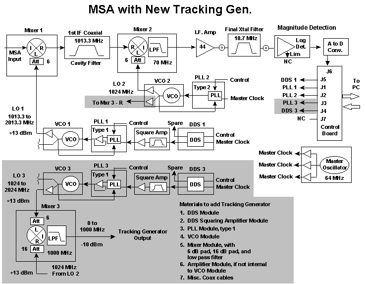
Tracking Generator Addition to the MSA :
The addition of
the Tracking Generator to the basic
MSA, satifies the VNA requirement of creating it's own test
signal. In the VNA, the Tracking Generator is also called the
Magnitude
Reference Generator. There are two design
options for the Tracking Generator, however, the
New Tracking Generator is the better choice for use with the VNA. The New
Tracking Generator option, used in the VNA, is shown in the following
MSA/VNA block diagrams.
Magnitude Reference Generation using the
New Tracking Generator:
Details of
construction can be found on the Tracking
Generator page.
In this scheme,
the Tracking Generator's Local Oscillator (LO 3) changes frequency at
the same rate as the MSA's tunable LO 1. The MSA's LO 2 (1024
MHz) is mixed with the TG's LO 3 to
create the Magnitude Reference Output (Tracking Generator Output of 0
MHz to 1000 MHz).
The actual frequency of the
Magnitude Reference output will not be
exactly the frequency of the MSA command. But, it will be within
a few
Hz. This is due to DDS accuracy.
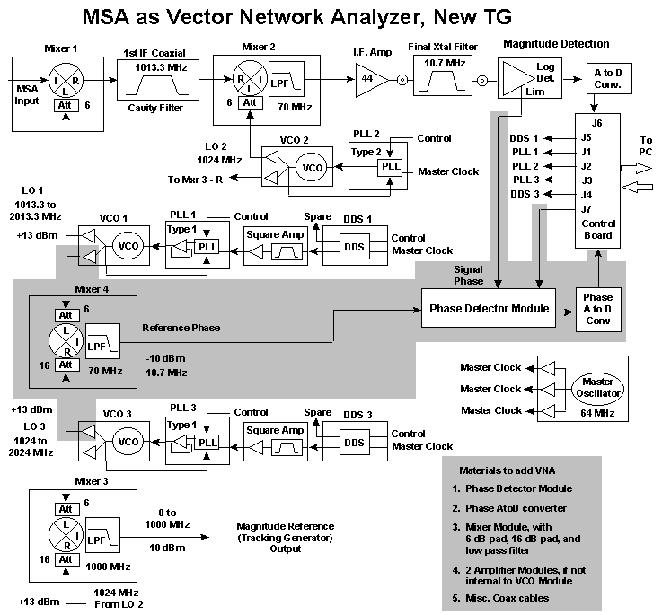
Phase Modification of MSA/TG :
Now that the
MSA has a Magnitude Reference (the New Tracking Generator),
the final addition can be made for VNA conversion. This is the
Phase
Modification ,and consists of two parts, the Phase Reference Generator
and
the Phase Detector. When these two items
are added, the MSA/TG becomes, MSA/VNA. I use the dual name,
because the MSA functionality is not deleted. Once built, the
software will tell the MSA/VNA what type machine it is.
The Phase Detector Module will be shown
after the description of the Phase Reference Generator.
MSA/VNA
Block
diagram of the MSA/VNA, using New
Tracking Generator as Magnitude Reference Generator: Block Diagram of
complete MSA /VNA
Phase
Reference Generation using the New Tracking Generator:
Since I recommend the New Trk. Gen. for Magnitude
Reference Generation, I show only one method for
Phase Reference Generation. It adds the Mixer 4
Module. It's output frequency will be the exact same
frequency as the
Final I.F. frequency of the MSA/VNA. The MSA's
frequency agile LO 1 is
mixed with the frequency agile LO 3 of the New Tracking
Generator. When the MSA is sweeping, LO 1 is changing from 1013.3
MHz to 2013.3 MHz. The software will command the LO 3 to track LO
1, but, with a difference frequency equal to the Final I.F.
frequency. The Mixer 4 product of 10.7 MHz is the Reference Phase
Signal.
Mixer 4 is labeled:
Mixer 4 (Mixer 3 B). This is because Mixer 4 is identical to the
Mixer 3B that is described on the Tracking Generator page. Just
duplicate the Mixer 3B for use as Mixer 4.
This Reference Phase Signal
will deviate in
frequency and phase when the MSA is being swept. But, that is not
important, and can be explained in the next paragraphs.
Signal Flow in the MSA/VNA :
The Magnitude
Reference output is directed to the Device Under Test. That
signal is sent either, through the DUT, or is a reflection from the
DUT. In either case, the signal is brought to the input of the
MSA/VNA. This signal contains the Magnitude and Phase change
caused by the DUT. It is converted, first to 1013.3 MHz by Mixer
1 and then converted to the Final I.F. of 10.7 MHz by Mixer 2.
The Final I.F. is filtered by the Final Xtal Filter and sent to the
Log. Detector. The Log Detector does two things. It
measures the Magnitude of the signal, and also diverts the I.F. signal,
as an RF Limited output, to the Phase Detector Module (PDM). This
Limited output is called the Signal Phase. Only the phase of this
signal is used by the Phase Detector Module. I highly suggest
using the AD8306 design for the Log Detector Module.
The Reference Phase signal from Mixer 4 is sent to
the Phase Detector Module for comparison with the Signal Phase.
The PDM will measure the difference in phase between the two signals
and will, eventually, become the DUT's Phase Vector. Without any
type of calibration, the Magnitude from the Log. Det. and the Phase
Vector from the PDM are meaningless. They are, simply, absolute
numbers without a reference. Once the MSA/VNA is calibrated, the
Magnitude output is numerically compared to a known calibration table
and the result becomes the DUT's Differential Magnitude. Same for
the Phase Vector. All about calibration techniques, later.
Now, I only will explain why a Reference Phase Signal deviation is not of concern. I know I
will be asked why.
I stated that, the Reference Phase signal will be exactly the same
frequency as the Final I.F. This can be explained with some
mathmatics, and should be easy to follow.
Let's call the frequency of the Magnitude Reference Signal, "M".
We will call the Reference Phase Signal "R".
The M signal goes through, or is reflected from the DUT, into the input
of the MSA/VNA. M now becomes the input to the MSA chain and gets
converted to the Final I.F. frequency. Call this FIF. The
formula for frequency conversion in the MSA is : FIF = LO2-(LO1-M).
The Reference Phase Signal, R = LO3-LO1
The Magnitude Ref Signal, M = LO3-LO2.
Simplify
the formula, FIF = LO2-(LO1-M) to FIF = LO2-LO1+M
Substitue M with (LO3-LO2). FIF = LO2-LO1+(LO3-LO2). FIF = LO2-LO1+LO3-LO2. Since
LO2 and -LO2 cancel each other
out, FIF = LO3-LO1. Since R= LO3-LO1, then R = FIF.
With this in mind, let's see what happens when any of the Local
Oscillators change frequency:
If LO 2 changes frequency, it cancels itself out in
the formula: FIF = LO2-LO1+LO3-LO2
If LO 1 changes
frequency, both R and FIF will change frequency by the same
amount of the LO 1 change: FIF = LO3-LO1 and R= LO3-LO1
If LO3 changes frequency,
the same thing occurs. Both R and FIF will change
frequency by the same amount of the LO 3 change, remaining equal to
each other.
This is a self-balancing frequency conversion, and
by theory, any frequency change or even phase noise will not be
detected by the Phase Detector Module. This phase noise
cancellation is not quite true in
the VNA, due to the MSA having a Final Xtal Filter and the Reference
Phase signal not having one. Very low frequency and phase change
will cancel out and will not be detected, but any phase noise greater
than the bandwidth of
the Final Xtal Filter will be detected by the PDM. However, the
PDM will have an output filter that will integrate the noise and the
phase measurement will not be sorely effected.
One other note: The Master Oscillator does not
need to be precise. However, it does need to be stable in
frequency.
The actual frequency of the Master Oscillator is entered into the
software by the user. Then, the software program will calculate
the actual frequencies of the system.
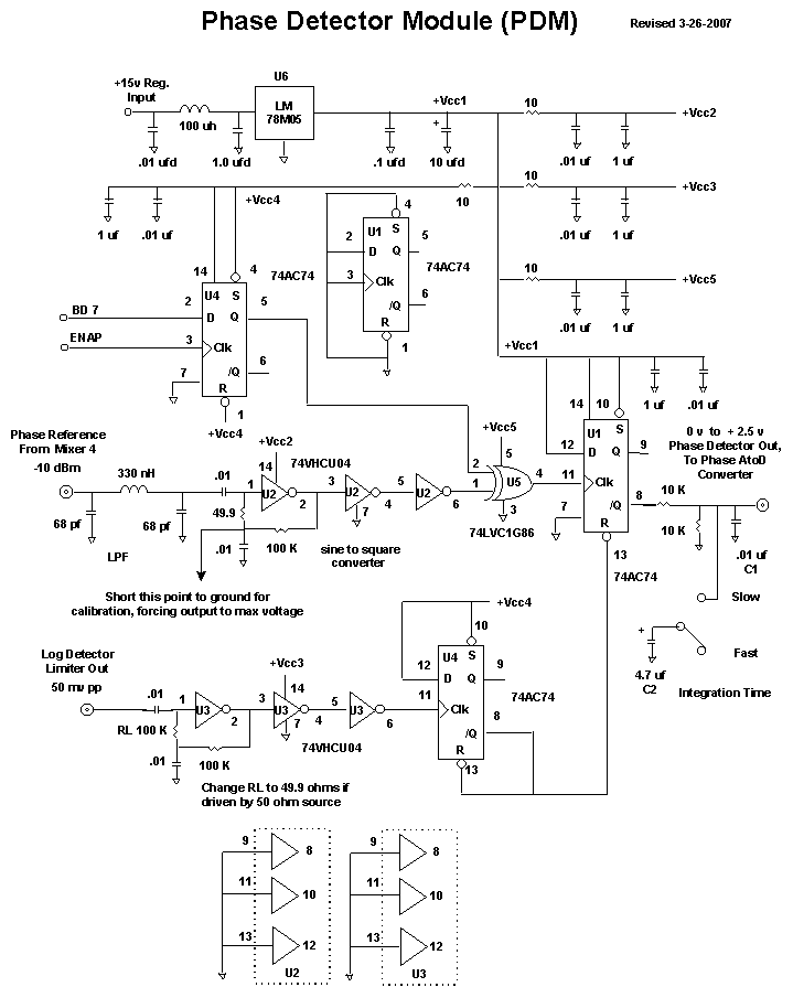
Adding the Phase Detector Module :
The MSA's Final I.F. is proposed
to be in the 10.7 MHz range. Of course, the MSA can be designed
with other I.F. frequencies, but the following phase detector design
will not work very well at frequencies greater than about 12 MHz.
By substituting higher frequency (faster) parts, it's operation could
be
extended well above 40 MHz. Other designs for a Phase Detector or
Phase Discriminator could be used. The requirements are: It
must be a 360 degree detector. The software is written
specifically to look for 0 degree and 360 degree dead zones for
automatic phase inversion. It must be linear. There is no
provision in the software for linearity calibration.
Schematic of Phase Detector Module for MSA/VNA :
This PDM is a very simple, yet highly accurate phase
detector
(discriminator). The linearity is precise enough that a software
calibration table is unnecessary. Parts are cheap and plentiful,
and substitutions are allowed. There are a few important aspects
when laying out and constructing this module.
Originally,
I showed an impedance matching circuit that converted the 50 ohm driver
impedance to a 1.5 K ohm load resistance. This increased the
voltage significantly for better driving margin. However, the
tuned circuit was very temperature sensitive, causing excessive phase
movement over temperature. Since ample driving power is supplied
by Mixer 4 (Phase Reference signal), I concluded (after testing) that
the extra voltage gain was not necessary. The low pass
filter is used instead of the original matching circuit. This
will also prevent high frequency interference to the
buffer, U2. Updated Mar 26, 2007 U1 is used as a
360 degree phase detector. For
excellent linearity, it's 5v supply should be very solid and well
bypassed at the Vcc, pin 14 to ground. All other devices that are
using +5v should be isolated
from the Vcc1, used at U1. Use about 10 ohms of series resistor
for every other Vcc. Do not use the
spare gates in U1, U2 or U3 for any other dynamic activity. They
will load the IC's internal Vcc bus and degrade the linearity. Do
not
"daisy chain" the other Vcc's. Connect their Vcc's directly
to the Voltage regulator. Position U1 and the Phase Detector
Output connector on one side of the module, away from all other
devices, except the Voltage Regulator. This will prevent the
ground
currents of the other devices from running the same path as the ground
current for U1. The easiest way to do this is build up the
Voltage regulator in one corner of the module and build U1 very close
to it. Build the other circuits on the oposite end of the board,
along with the input connectors. This sounds like a lot of work,
but careful planning will result in extremely good phase detection
linearity. When I get a chance, I will photograph my module (dead
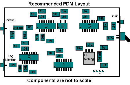
bug style) and post it here. Included here, is a recommended
layout. This layout will minimized ground loops, which will cause
unlinearity. The components are not to scale, and the board can
be made very small.
The RF Limited Output of the Log
Detector (AD 8306) is already a square wave, and sourced as 50
ohms. The Phase Reference input has a 50 ohm low pass
filter. As in the other modules built for the MSA, this module
must be totally enclosed in a shielded container. I have fine
results using the 74 VHCU 04, but I'm sure the HCU 04, will work,
too. The purpose of the 74LVC1G86 is to invert the signal,
creating a 180 degree phase shift. In reality, I guarantee it
will not be exactly 180 degrees, but, the difference is "remembered"
during calibration.
A power connector with the 2 signals, BD7 and ENAP
is advised, keeping a seperate SMA output connector for the Phase
Detector Output to the AtoD converter. The Control Board needs a
modification to add a connector containing the 2 signals, along with
power and ground. This will become Control Board, J7.
Note: The value of C1 is nominally, .01
ufd. This sets the integration time of the PDM output and is
subject to change as I determine the best integration time for the
software. My PDM Output has a peak to peak noise value of about
15 mv. This noise creates an error of approximately 2
degrees. Increasing C1 to about 4.7 ufd will integrate the peak
to
peak noise to about 1 mv, and allow an error of only .17 degrees.
However, the sweep must be slowed to a crawl, to utilize this very high
integration time (increase the "Wait" box value).
Phase Detector Module Description and
Operation:
The Phase
Reference
signal is filtered, buffered, and amplified into a square wave (U2),
and sent to the input of the exclusive OR gate, U5. The other
input of the XOR gate can be toggled by the software to invert the XOR
output. This is how a 180 degree inversion is accomplished.
The XOR output is used to
trigger U1 (positive edge). This is the "start" signal
at U1-11.
The RF Limited
signal from the Log Detector is buffered and amplified into a square wave
(U3), and
used
to trigger U4 (positive edge). This creates the "stop"
signal at U4-11. "Stop" creates a negative going pulse, about 5
nsec
wide, at U4-8. "Stop" causes U1 to clear (U1-13) with U1-8 (/Q)
going to a
logical "1".
U1-8 (/Q) is a
square wave, with a duty cycle that
is proportional to the time of "start" to "stop". A resistive
divider (10 K) halves the 5 volt, maximum /Q voltage to 2.5 volts for
the AtoD converter. The capacitor, C1, is the integrator, to
convert the duty cyled square wave into a smooth DC voltage. C1,
and the resistive divider, determines the bandwidth of the PDM.
If there is no "start" signal from the Phase
Reference, and there is a
continuous "stop" signal (from the Log Detector Limiter), the PDM
output will remain
at a nominal, + 2.5 volts. A shorting point at the Phase
Reference input
buffer (U2) is provided to accomplish this action. With a stable
+ 2.5
volt PDM output, the AtoD converter can be adjusted for maximum bit
count. The software uses this bit value as a 0/360 degree
reference.
For example, if the PDM supplies +2.5 volts to the
Phase AtoD, the AtoD will create a Bit count of 4095 and the software
will use 4095 as a
360 degrees (0 degrees) reference point. It will convert +1.25
volts to a bit count of 2047 Bits, equating to 180 degrees, and +.625
volts to 90 degrees,
etc. 0 volts is converted to 0 Bits and is used as 0 degrees
(also 360
degrees).
This type of phase detector operates in the time domain. If the
"Start" and "Stop" signals are very close together, U1 will trigger
erratically, due to non-linearities and
FF "uncertainties". This is called the "dead
zone". Due
to time delays in the U1 and U4 flip flops, there can be a significant
"dead zone". This is the time the data will be invalid. The software will "look"
for this area of
uncertainty.
In my circuit,
I am using 74AC74's for the FF's. The "dead zone" is about
7
nsec wide. At 10.7 MHz, 7 nsec equates to about 27 degrees.
The 0/360
degree point is not in exactly in the center of the "dead zone".
Therefore, the software will add some margin to guarantee that the PDM
will not take data near the "dead zone". The software will
consider data to be valid if the PDM output voltage is between 20% and
80% of the maximum output voltage (2.5 volts). At 10.7 MHz, this
equates to about 216 degrees of valid area and 144 degrees of invalid
area. This is more than enough margin to guarantee the data
acquision will not be close to the "dead zone".
This software margin is wide enough to allow using the 74HC74 or HCT74,
probably the slowest anyone will ever use. Builders using faster
FF’s will have an
even better margin.
The Analog to Digital Conversion Process :
The MSA can be
built with a choice
of 3 different A to D conversion schemes. Any of them will
work. Since the 8 bit AtoD is only 256 bits, the resolution
of Phase Detector measurement is equal to 360 deg / 256 = 1.4
degrees per bit. This is not enough resolution for
superior vector measurements, but it will get you in the
"ballpark". The 12 bit AtoD is 4096 bits, the
per-bit resolution
of Phase Detector measurement is equal to 360 deg / 4096 = .088
degrees. Since the AtoD will measure down to +/- 1 bit this
equates to an error of .176 degrees. This is more than adequate
for excellent phase
measurements. The serial 16 bit AtoD could, in theory, have a
per-bit resolution of 360 deg/65536 = .0055 degrees. In reality,
the phase resolution of the VNA will be about 1 degree, due to the
inherent phase noise of the basic MSA.
Calibration
of the MSA/VNA :
Other than the standard calibration required for MSA operation, there
are two calibrations required for VNA operation.
PDM Output Level
Calibration. The PDM's maximum output is
nominally 2.5 volts for a 360 degree phase shift, but will vary a minor
amount due to the actual +5 volts of the internal voltage
regulator. The AtoD is
adjusted for maximum bit conversion for the PDM Output voltage.
Proceedure, after 30 minute warm-up:
No external signal is needed on the input of the VNA (MSA Input).
RUN the
Spectrum Analyzer program from the Code Window, it starts sweeping in
the MSA Mode. Halt the sweep, by pressing any letter on the
keyboard.
Click
the "Go-VNA Mode" button. It now begins sweeping in the VNA
Mode. Halt the sweep.
Click
the "Track Gen is OFF" button to turn on the Tracking Generator.
Enter 0 (MHz) into the "Center Frequency" box and 0 (MHz) into the "Sweep Width" box.
Click
"RESTART". The Graph Window will probably plot a ramp waveform
but since the AtoD is not calibrated yet, the waveform is
meaningless. Halt the sweep.
Click the "Show Variables" button to open the "Variables" window.
In the
"Variables
Window" find the value of "Pha AtoD Bits".
Click the "CONTINUE" button. Sweep will resume and the "Pha AtoD Bits" in the "Variables
Window" should be changing value.
Short
the calibration point
in the Phase Detector Module to ground. This causes the PDM to
output it's maximum voltage (for 360 deg). The Graph Plot will
probably go very erratic, but this is normal. Adjust the Phase
AtoD
Converter's adjustment pot while watching the value of "Pha AtoD Bits". Adjust for one or two bits less
than the possible maximum (example, 4093, out of 4095, for the 12 Bit
converter). Halt sweep and enter this value in the Code Window,
global variable,
"maxpdmout" = 4093 (your final bit value). "Save" your code with
this new value. Remove the short inside the PDM. This is a one time calibration,
and should never have to be repeated if no changes are made to the PDM
or AtoD converter.
PDM Phase Inversion
Calibration. This
calibration is for determining the actual phase shift of the PDM when
it is inverted 180 degrees. I can assure you, it will not be
exactly 180 degress, due to the internal differences in chip delays.
Perform this calibration AFTER
the PDM Output Level Calibration is performed.
Proceedure, after 30 minute warm-up:
Connect a two to three foot long, 50 ohm test cable from the Reference
Output (Trk Gen Out) to
the VNA Input (MSA Input). Make sure you don't overdrive the
input. If necessary, add some padding to keep the level of the
input below the maximum input power level.
RUN the
Spectrum Analyzer program from the Code Window, it starts sweeping in the MSA
Mode. Halt the sweep.
Click
the "Track Gen is OFF"
button to turn on the Tracking Generator. Button will change to
"Track Gen is ON".
Click
the "Go-VNA Mode" button. It now begins sweeping in the VNA
Mode. The button will change to "Go-MSA Mode". Halt the
sweep.
Enter 200
(MHz) into the "Center Frequency" box and 350 (MHz) into the "Sweep Width" box. These
values are not important, we just want at least one full ramp waveform
when sweeping.
The "PDM Inversion" box will show "180". This is a software
default for the Global Variable, "invdeg". You could change this
value to anything between 0 and 360, except, "1". This value
will "tell" the software what the actual PDM phase inversion is, in
degrees. Entering a "1" here will tell the VNA to automatically
determine the phase inversion, in degrees. For the moment, leave
it at "180".
Do not click the "Calibrate ?" button.
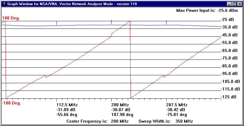
Click "RESTART". The Graph Window and plots should look similar
to this:
Verify at least one full ramp
waveform. What occurs is, the time
delay through the MSA/VNA is enough to cause the two signals to the
PDM, to change relative phase by more than 360 degrees. You
should
see that the linear portion of a full ramp has two small level
shifts. This is where the PDM is being
commanded to invert (to create a 180 degree phase shift). The
visible level shift is the difference in 180 degrees and the actual
phase shift. If this shift is not very noticeable, your PDM is
very close to having a real 180 degree shift. If so, halt the
sweep and insert the value, "170" or "190" into the "PDM Inversion" box. Click
"RESTART" and observe a larger level shift.
Halt the sweep.
Place the mouse pointer directly on the small level shift transition of
the plot. Left click the mouse. The frequency, at which
this level shift occurs, will automatically enter the "This Freq" box.
Click the "Cent" box. The frequency will
automatically enter the "Center Frequency" box.
Enter "0" into the "Sweep Width" box.
Click
"RESTART". The swept phase response will be a flat line (with
some noise possible) corresponding to a stationary phase differential
at the inputs to the PDM. Since the frequency is not changing,
the phase will not change, either.
Halt the sweep.
Enter the value, "1" into the "PDM Inversion" box. This
will tell the VNA to calibrate for "invdeg".
In the PDM, switch in the extra 4.7 ufd of capacitance (C2) with the
integration capacitor, C1. This will minimize noise to the AtoD
for accurate calibration.
Click
"RESTART". The computer will "beep" and the PDM is commanded to
"Normal", no inversion. Phase data is taken after a long
wait period. Then, the PDM changes from normal to invert, and Phase data is taken again, after a
another long wait period. The two data values are compared, and
the actual phase change value is calculated. The value
inside the "PDM Inversion" box will change
from "1" to this calculated value of phase inversion, in degrees (a
negative value is ok). Mine
is 182.2 degrees. The computer will beep again, and
the "Hit any key" box will show the word, "cald" (the PDM phase
inversion is now, calibrated). Repeat the process a few times.
Insert "1" into the "PDM Inversion" box and click
"RESTART". Verify the phase in the "PDM Inversion" box is consistant,
to within about .2 degrees (for the 12 bit AtoD).
Halt
sweep and enter this value in the Code Window, global variable,
"invdeg" = 182.2 (your actual value). "Save" your code
with this new value. This is a one time calibration,
and should never have to be repeated if no changes are made to the PDM.
Operation of the VNA :
RUN the
Spectrum Analyzer program from the Code Window, it starts sweeping in the MSA
Mode. The
Working Window of the MSA software has a button called: "Go-VNA
Mode".
Click this button and the MSA will enter the VNA mode of
operation. Sweeping will begin with the latest parameters entered
in the MSA mode. The button will change its name to, "Go-MSA
Mode". Use this button to return to the MSA mode of
operation. If the Tracking Gen is "OFF", halt the sweep and click
the button for "Track Gen is ON". Restart the sweep.
There will be two plots in the Graph Window. A
blue plot showing the magnitude (power) of the input signal, with its
scale on the right side. And, a red plot showing the phase of the
input signal, with its scale on the left side. The MSA Input and
VNA Input are the same points, ie, the input to Mixer 1.
Until the VNA is "Calibrated", both signal plots are
not relative to the Magnitude Reference Output (Tracking Generator
Output). The magnitude plot will read absolute power of the
Input, exactly the same as when in the MSA Mode. Restated, it is
power, relative to 0 dBm. The phase plot will be the approximate phase
difference
of the two signals entering the Phase Detector Module (PDM). If
there is no input to the VNA (Reference not connected to Input), the
Phase plot will be random. For the two plots to become relative
to the Mag Ref Out, the user must perform a Line Calibration.......the
"Calibrate ?" button.
Line Calibration:
When measuring
parameters of a Device Under Test (DUT), the internal delays of the VNA
and external delays of the test cables must be factored out of the
results. A Line Calibration will achieve this. Connect the
Reference Output to the VNA Input using a short 50 ohm cable, 1 to 3
foot in length. The Reference output will have a nomimal power
level of -10 dBm. For most accurate VNA results, it is best for
the input
signal to be less than 10 dB below the Max Power Input to the
VNA. Use a 10 dB attenuator attached to the Input and another 10
dB attenuator attached to the Ref Output. Use more attenuation if
necessary. In the Working Window, enter the parameters for the
frequency range of interest. Click the "Calibrate ?" button. The
button will change to "Calibrating" and the sweep will start .
The two plot lines will align on their respective "0" reference
positions. The Magnitude plot line will be at the very top of the
graph, if the Magnitude scale (on the right) begins below 0 dB.
The Phase plot line will be in the center of the graph. The
single sweep will terminate with a "beep" from the computer. The
button will now change to "Calibrated". The word "end" will
display in the "Halt sweep" box. The VNA is now calibrated.
All further sweeps will be relative to the information taken during
this Calibration sweep. The Magnitude plots will be in dB
relative to the Calibrated Sweep. The Phase plots will be in
Degrees relative to the Calibrated sweep. The VNA can be
re-calibrated, at any time, by clicking the "Calibrated" button.
When the MSA/VNA is commanded into the MSA mode or
into the VNA Mode, the Line Calibration table is cleared of all
contents. So, the calibration table can be cleared by entering
the MSA Mode and re-entering the VNA Mode.
Software for the MSA/VNA : The Software for the MSA/VNA is
written in Liberty Basic, download
spectrumanalyzer.bas
Screen
Plots of the MSA/VNA :
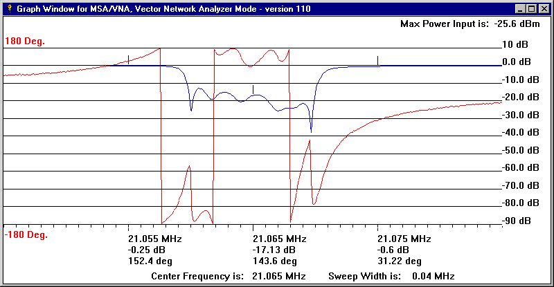
This is a screen shot of a 21.065 MHz Crystal Filter with a bandwidth
of 11 KHz. As an S parameter measurement, it is S21 (insertion
loss and phase change through the filter).
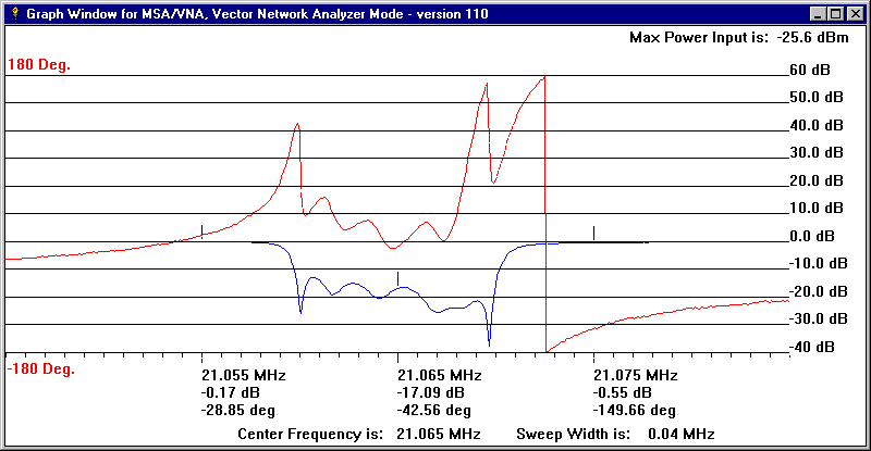
The following is a screen shot of the reflection of same filter using a
power divider as a reflection bridge. Calibrated with bridge open.
The
following is a screen shot of the reflection of same filter with the
bridge calibrated with a short. Notice the phase has shifted
from the above plot, by about 180 degrees. The actual delay of
the bridge has not been calibrated or factored into the data. The
power reference scale
was shifted to allow better clarity of the two plots.