Using a Step Recovery Diode
or Snap Diode
This
Page was Started Dec. 18,
2004
Updated 1-25-05, add link for CAD layout of SRD board
Updated 2-25-11, Update this page.
This page will act as a design guide for building a frequency multiplier using a diode that has a long Carrier Lifetime and short Transition Time. Some diodes that exhibit these qualities are Step Recovery Diodes, Varactor Diodes, and PIN Diodes. This page uses the terms SRD, Snap, and PIN Diodes randomly, but they all mean the same thing. I did not design this multiplier for maximum efficiency. Had I done so, the input and output would be specific (64 MHz X16 = 1024 MHz). The circuits and components would be extremely critical, and the layout topology would probably be impossible to duplicate. So, if you say "that doesn't look like any multiplier I have ever seen", you are right. However, this scheme will work with different frequencies and different multiplication factors other than just 64 MHz and X16.
My original intention was to build a frequency multiplier for the Modularized Spectrum Analyzer. The MSA's 2nd Local Oscillator, which runs at 1024 MHz, is a PLL/VCO/Amplifier combination. There is absolutely nothing wrong with that scheme, but it can be replaced with this SRD multiplier scheme to improve Spectrum Analyzer phase noise results. The total SA phase noise improvement is only about 1 dB. Therefore, using a multiplier scheme for LO 2 has no benefit unless the SA's LO 1 is modified for low phase noise operation.
At the end of this page is some technical information for Step Recovery Diodes.
Go back to the MSA Main Page
Frequency Multiplier Block Diagram to replace PLL2 and VCO 2:
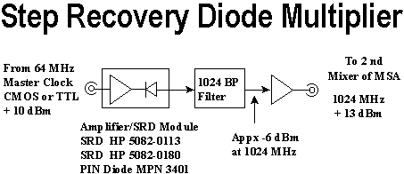
This frequency multiplier scheme consists of a driver, impulse generator (Snap Diode), filter, and an amplifier. The filter is a coaxial cavity filter tuned to 1024 MHz and an insertion loss of 1.5 dB. The amplifier has approximately 20 dB of gain and is saturated with an output of about +13 dBm. In the following diagram, the driver and impulse generator are combined onto one pwb.
The Driver, the Step Recovery Diode Module
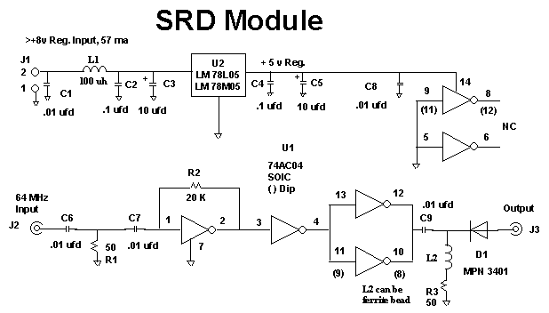
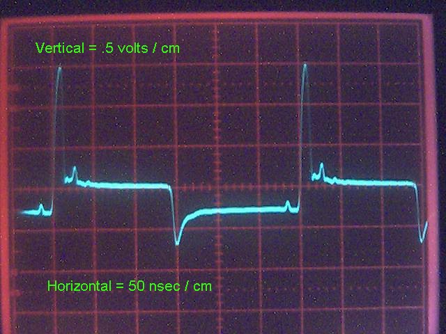
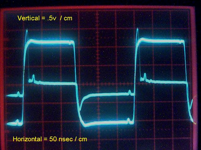
This module can respond to a sine input, but it is expected to receive the square CMOS signal from a 64 MHz Master Clock. The first section of the 74AC04 (or ACT04) will convert the input. The second stage will square up the signal. The third stage is a parallel driver, to assure maximum drive to the Snap Diode. The Snap Diode acts as the impulse generator. Notice that the Snap Diode is not a Step Recovery Diode, but rather, a PIN diode (MPN 3401). Although not as efficient as an SRD, this particular PIN diode performs well in this design. It is also extremely cheap and available (about 50 cents, compared to about $20 for an SRD). The completed multiplier measures only 3 dB less efficient than when using the HP 5082-0113, an SRD.
R3 is the self bias resistor for the PIN. Although its value is shown to be 50 ohms, it will be changed to optimize the circuit efficiency or accomodate different SRD's. Notice, there is no load or resonator on the output of D1. A resistive or inductive load must be shunted at J3 for the diode to function. A 50 ohm load could be placed at J3 to create a "Comb Generator". But for this application, the hairpin input of the cavity filter will act as an inductive load for the SRD.
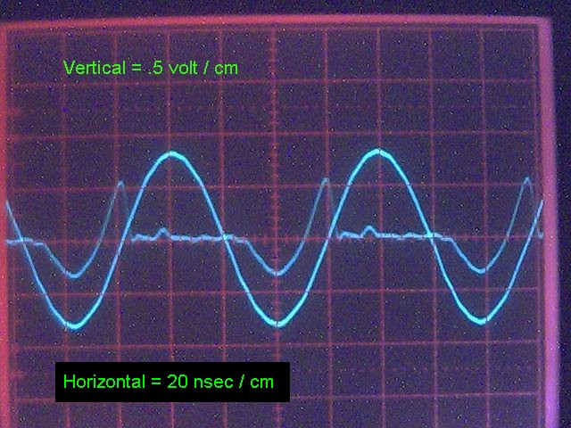
The actual measured output of the SRD module (as a comb generator) is approximately -23 dBm at 1024 MHz. When the resistive load is replaced with the band pass filter, the filter's output power is -5 dBm at 1024 MHz. I realize that this sounds like voodoo reverse-conservation of energy, but the band pass filter acts as a reflector to all harmonics except the one at 1024. The reflected harmonics are directed back to the SRD and their combined power will increase the efficiency of the SRD action.
The Snap Diode can be mounted in either direction. I found that maximum power output was obtained with the diode's cathode on the output. This is not due to the effeciency of the diode. It attributed to the '04 driver, which has more current capability on its negative edge than its positive edge.
Changing the bias resistor will change the length of time that reverse current is supplied to the diode. This does not change carrier lifetime of the SRD, but it does change the total circuit lifetime. This changes the circuit efficiency. Using various resistor values, the filter's output power can be maximized. The actual resistor value depends on many factors, but it should be between 200 ohms and 2000 ohms. After much "resistor tweeking", my final bias resistor value was 1.1 K ohms.
Power could be further increased by using a specific length delay line between the SRD output and the input to the cavity filter. A critical phase delay would allow the reflections from the filter to affect the SRD efficiency. This delay line technique could possibly result in a power output of +6 dBm. However, this is below the requirements for the mixers in the MSA, so a post amplifier is needed.
Without the delay line an output from the filter might be as high as +2 dBm, but a more conservative expectation is somewhere between -6 dBm and 0 dBm. Since an amplifier is required for either topology (with or without delay line), I chose not to include the delay line in the design. Its length is extremely critical, anyway. An amplifier can increase the total power to drive any mixer.
Here are screen shots of the SRD Module Board Layout. I used ExpressPCB software, which can be accessed by clicking, SRD Module PWB. The size of the board is 1.4 x 1.35 inches (this does not conform to present SLIM requirements). Layer 1 is the silkscreen, layer 2 is the top copper, layer 3 is the bottom copper (as seen from top) :
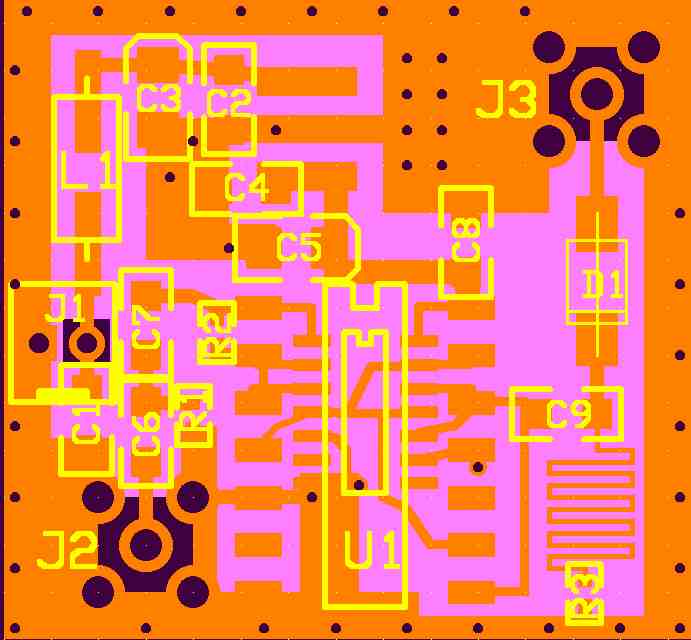
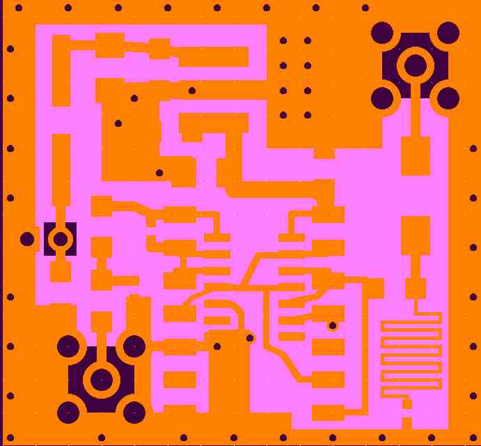
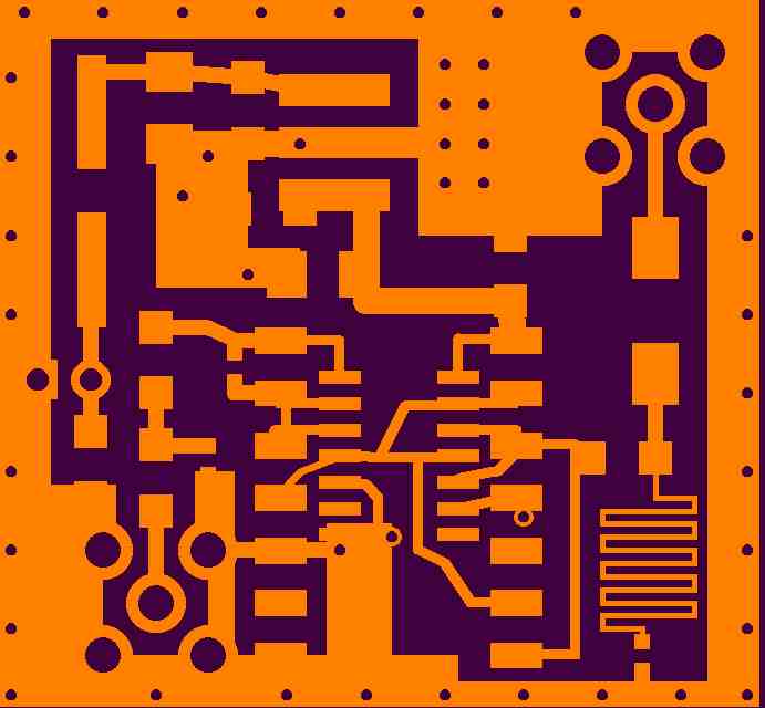
Click for : all Layers, Layers 2 and 3, Layer 2,
The board is layed out so that either the DIP or SOIC package 74AC04 can be used. I used the SOIC for testing.
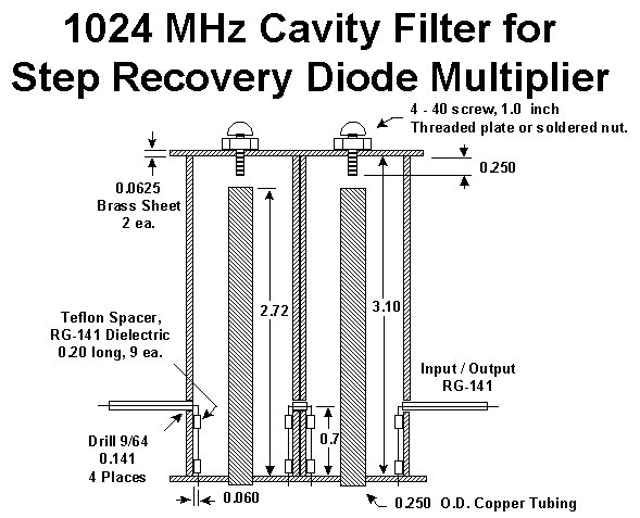
1024 MHz Dual Cavity Filter, dimensions are inches.
Updated 1-25-05, add link for CAD layout of SRD board
Updated 2-25-11, Update this page.
This page will act as a design guide for building a frequency multiplier using a diode that has a long Carrier Lifetime and short Transition Time. Some diodes that exhibit these qualities are Step Recovery Diodes, Varactor Diodes, and PIN Diodes. This page uses the terms SRD, Snap, and PIN Diodes randomly, but they all mean the same thing. I did not design this multiplier for maximum efficiency. Had I done so, the input and output would be specific (64 MHz X16 = 1024 MHz). The circuits and components would be extremely critical, and the layout topology would probably be impossible to duplicate. So, if you say "that doesn't look like any multiplier I have ever seen", you are right. However, this scheme will work with different frequencies and different multiplication factors other than just 64 MHz and X16.
My original intention was to build a frequency multiplier for the Modularized Spectrum Analyzer. The MSA's 2nd Local Oscillator, which runs at 1024 MHz, is a PLL/VCO/Amplifier combination. There is absolutely nothing wrong with that scheme, but it can be replaced with this SRD multiplier scheme to improve Spectrum Analyzer phase noise results. The total SA phase noise improvement is only about 1 dB. Therefore, using a multiplier scheme for LO 2 has no benefit unless the SA's LO 1 is modified for low phase noise operation.
At the end of this page is some technical information for Step Recovery Diodes.
Go back to the MSA Main Page
Frequency Multiplier Block Diagram to replace PLL2 and VCO 2:
This frequency multiplier scheme consists of a driver, impulse generator (Snap Diode), filter, and an amplifier. The filter is a coaxial cavity filter tuned to 1024 MHz and an insertion loss of 1.5 dB. The amplifier has approximately 20 dB of gain and is saturated with an output of about +13 dBm. In the following diagram, the driver and impulse generator are combined onto one pwb.
The Driver, the Step Recovery Diode Module
This module can respond to a sine input, but it is expected to receive the square CMOS signal from a 64 MHz Master Clock. The first section of the 74AC04 (or ACT04) will convert the input. The second stage will square up the signal. The third stage is a parallel driver, to assure maximum drive to the Snap Diode. The Snap Diode acts as the impulse generator. Notice that the Snap Diode is not a Step Recovery Diode, but rather, a PIN diode (MPN 3401). Although not as efficient as an SRD, this particular PIN diode performs well in this design. It is also extremely cheap and available (about 50 cents, compared to about $20 for an SRD). The completed multiplier measures only 3 dB less efficient than when using the HP 5082-0113, an SRD.
R3 is the self bias resistor for the PIN. Although its value is shown to be 50 ohms, it will be changed to optimize the circuit efficiency or accomodate different SRD's. Notice, there is no load or resonator on the output of D1. A resistive or inductive load must be shunted at J3 for the diode to function. A 50 ohm load could be placed at J3 to create a "Comb Generator". But for this application, the hairpin input of the cavity filter will act as an inductive load for the SRD.
The actual measured output of the SRD module (as a comb generator) is approximately -23 dBm at 1024 MHz. When the resistive load is replaced with the band pass filter, the filter's output power is -5 dBm at 1024 MHz. I realize that this sounds like voodoo reverse-conservation of energy, but the band pass filter acts as a reflector to all harmonics except the one at 1024. The reflected harmonics are directed back to the SRD and their combined power will increase the efficiency of the SRD action.
The Snap Diode can be mounted in either direction. I found that maximum power output was obtained with the diode's cathode on the output. This is not due to the effeciency of the diode. It attributed to the '04 driver, which has more current capability on its negative edge than its positive edge.
Changing the bias resistor will change the length of time that reverse current is supplied to the diode. This does not change carrier lifetime of the SRD, but it does change the total circuit lifetime. This changes the circuit efficiency. Using various resistor values, the filter's output power can be maximized. The actual resistor value depends on many factors, but it should be between 200 ohms and 2000 ohms. After much "resistor tweeking", my final bias resistor value was 1.1 K ohms.
Power could be further increased by using a specific length delay line between the SRD output and the input to the cavity filter. A critical phase delay would allow the reflections from the filter to affect the SRD efficiency. This delay line technique could possibly result in a power output of +6 dBm. However, this is below the requirements for the mixers in the MSA, so a post amplifier is needed.
Without the delay line an output from the filter might be as high as +2 dBm, but a more conservative expectation is somewhere between -6 dBm and 0 dBm. Since an amplifier is required for either topology (with or without delay line), I chose not to include the delay line in the design. Its length is extremely critical, anyway. An amplifier can increase the total power to drive any mixer.
Here are screen shots of the SRD Module Board Layout. I used ExpressPCB software, which can be accessed by clicking, SRD Module PWB. The size of the board is 1.4 x 1.35 inches (this does not conform to present SLIM requirements). Layer 1 is the silkscreen, layer 2 is the top copper, layer 3 is the bottom copper (as seen from top) :
Click for : all Layers, Layers 2 and 3, Layer 2,
The board is layed out so that either the DIP or SOIC package 74AC04 can be used. I used the SOIC for testing.
The
Band Pass Filter
The following dual coaxial cavity filter can be used as the band pass
filter, to pass the 16 th harmonic of the SRD's 64
MHz input. I won't repeat the build process on this page.
For pictures and construction techniques, go to the Cavity Filter
page. This dual filter can be replaced with other narrow band filters
with good results. I have done extensive
multiplier testing using a single coaxial cavity filter
instead of this two stage coaxial cavity filter. The 15th and 17th
harmonics (960 MHz and 1088 MHz) are attenuated about -30 dB below 1024
MHz, which is adequite for use in the MSA.
1024 MHz Dual Cavity Filter, dimensions are inches.
