MSA with Tracking Generator, and VNA using
Standardized Lab Integration Modules (SLIMs)


Updated 11-20-10: Engineering Change Notice, see SLIM-PDM Revision C, addition of 2 capacitors.
Updated 2-24-11: Add optional Amplifier to increase reverse isolation between Mixer 3 and PLO 2.
Updated 11-29-11. Updated the Wiring Diagram to Rev D, to include new optional modules
Updated 12-12-12. Clean-up page
Updated 12-20-14. Clean-up instructions in paragraph: 16 Bit Serial A to D Converter
Updated 1-27-15. Add advisory to PLO1 and PLO3
Updated 1-24-16. Clean-up page
Updated 9-12-16. Add paragraph when using SLIM-ADCMUX
Updated 11-15-16. Add SLIM-ADCMUX and optional RF Switch to Modules List
This page will suggest methods to integrate the SLIM MSA using block diagrams, a list of required modules, and a recommended layout. The SLIM MSA is functionally identical to the Original MSA, but constructed using SLIMs. Readers who have built, or are in the process of building the Original MSA using modules that are not specifically SLIMs, may still use this page as a guide. I am concentrating on the SLIM MSA, but it does not obsolete my Original MSA design. The Original MSA will continue to be supported in the software. If you are interested in building only the Basic Spectrum Analyzer, simply disregard the additional requirements to add the Tracking Generator or VNA modules.
This page will not detail the construction of each SLIM. Those construction details are on each SLIM's web page. Those pages describe the SLIMs in detail, including links to full documentation.
Modules List, SLIMs required to integrate the MSA systems:
It is suggested that the following SLIMs be constructed in the sequence that they are listed. That way, the long term builder can gain satisfaction by testing each SLIM as it is constructed. See Test-As-You-Build, a test procedure for SLIMs as they are built and integrated into the MSA. Or, the builder can complete his SLIM constructions and MSA Integration before testing. See Testing the Integrated MSA, a test procedure and troubleshooting guide for a fully integrated MSA. Click on any part number to link to that SLIM's web page.
Module Name Part Number
Control Board, SLIM-CB-NV
Phase Detector Module, SLIM-PDM (for MSA/TG/VNA, Level 3)
A to D Converter Module, SLIM-ADC-16 or optional SLIM-ADC-12 or optional SLIM-ADCMUX
Log Detector Module, SLIM-LD-8306
Master Oscillator Module, SLIM-MO-64
DDS 1 Module, SLIM-DDS-107 (and DDS 3 Module for MSA/TG, Level 2)
Final Crystal Filter (Resolution Bandwidth Filters). See SLIM page for optional filters (SLIM-MCF-xxxx or SLIM-CLF-xxxx).
Optional RF Switch SLIM-2P4T Path Switch for RBW Filters
Mixer 2, SLIM-MXR-2
Mixer 1, SLIM-MXR-1
Mixer 3, SLIM-MXR-3 (for MSA/TG, Level 2)
Mixer 4, SLIM-MXR-4 (for MSA/TG/VNA, Level 3)
PLO 2, SLIM-PLO-2
PLO 1, SLIM-PLO-1 (and PLO 3 for MSA/TG, Level 2)
First IF Filter, Coaxial Cavity Filter (technically, not a SLIM)
I.F. Amplifier Module, SLIM-IFA-33
Optional Buffer Amplifier, SLIM-RFA-1 (optional for MSA/TG Level 2)
The following items are additional, to complete the integration of the SLIM MSA, :
1. Metal enclosure, to house the MSA system.
For a completely portable MSA, the enclosure would be large enough to include a rechargeable 13.6 volt battery with enough capacity to supply the MSA and a Laptop Computer at the same time.
2. External power supply
The MSA/TG/VNA requires an input of +12 VDC to +15 VDC, with a typical current draw of 750 ma. (600 ma for Basic MSA). I caution the use of Switching Power Supplies. Even if the line regulation is supurb, the switching noise radiated into the air may interfere with the MSA operation. I have always suggested using a linear power supply. For lab use, a hefty (1 amp) "wall wart" will suffice. If the builder decides to incorporate an internal, linear power supply into the MSA, I give this warning: Use a magnetically shielded power transformer. Keep it as far away from the SLIMs as possible. Magnetic induction will show up as 60 Hz spurs (and harmonics).
3. Coaxial cables, to interconnect the SLIMs with RF signals or signals that need shielding.
I recommend RG-085 semi-rigid (hard pipe). There are several 50 ohm varieties of this style and size, so I will not be specific with part numbers. The interconnections are shown in the previous Block Diagram. Connectors are optional for cables and SLIMs. If used, SMA connectors are preferred.
4. Wire harness, to interconnect the SLIMs with power and command signals. I show a single wiring diagram for the MSA/TG/VNA (Build Level 3). Items using Notes 2. and 3. are not required when constructing the Basic MSA, and items using Notes 3. are not required when constructing the MSA/TG.
5. RF panel mount connectors
The MSA's RF panel mount connectors are not specified. They are a builder's preference. They only need a coaxial connection from the front panel to the bottom of the associated SLIMs. I like a type N on the front panel because it is extremely durable.
6. Parallel Port Interface Cable with DB25M connectors,
7. Cypress USB and USB cable when the optional USB is used.
Jump to major items on this page: (use browser BACK button to return here)
Block Diagram for MSA/TG/VNA
Wiring Diagram MSA
Layout of the MSA/TG/VNA using SLIMs
Special Instructions while integrating the MSA
MSA Specifications
Cost of the Basic MSA using SLIMs
Here are other links supporting the integration of the SLIM MSA:
SLIM Web Page. Description of the "SLIM System" and links to all SLIM construction pages.
Construction Techniques. Hints on constructing the SLIMs. Before beginning construction of the MSA, or any of the SLIM's, I highly suggest reading these hints. It may save you a lot of potential grief.
MSA Control and Operation. Basic operation, control and human interface for the MSA.
Set-Up and Calibration Procedures for the MSA. Instructions for downloading software, initial turn-on, calibration, and alignment for the MSA.
Technical Analysis of the SLIM MSA. Very handy for troubleshooting the MSA.
Express Printed Wiring Boards for the SLIM MSA, the Tracking Generator and VNA extension.
Integration Diagrams for the SLIM MSA
Block Diagram of SLIM MSA/TG/VNA
The labeled blocks within the following Diagram are Modules, or SLIMs, Standardized Lab Integration Modules. Each SLIM is a functional module, with specific properties. Some of the SLIMs require modifications for proper integration into the MSA. The Coaxial Cavity Filter is not considered a SLIM.
Block Diagram of SLIM MSA/TG/VNA

Notes:
* The optional Buffer/Amplifier between PLO 2 and Mixer 3 will reduce system RF crosstalk. Optionally, the builder can place a duplicate Buffer/Amplifier between PLO 1 and Mixer 4.
* A power supply is not shown, and for clarity, the interconnecting wiring harness is not shown.
* All of the inter-module connections shown, are coaxial cables. I recommend using RG-085, semi rigid cable for all module interconnections.
* There is no bandwidth limiting filter preceding the Mixer 1. This option is left up to the builder. With no filtering, the MSA will respond to all input frequencies, from DC to 3 GHz.
* The Tracking Generator Output has no filtering. Again, this is left up to the builder. With no filtering, the Tracking Generator will output a combination of frequencies (See the MSA Specifications).
* Both DDS 1 and DDS 3 have spare outputs (J3). I suggest connecting them to front panel connectors for greater MSA utility.
1. If configuring for the 1G Band of operation (0-1000 MHz) then arrange the coaxial interconnections in the following manner:
Input signal to MSA at Mixer 1, J2
Mixer 1, J3 to the input of the Coaxial Cavity Filter.
Mixer 2, J2 to the input of the I.F. Amplifier, J3
The Tracking Generator connections are: PLO3-J2 to Mixer3-J1. Mixer 3-J2 is output
2. If configuring for the 2G Band of operation (1000-2000 MHz) then arrange the coaxial interconnections in the following manner:
Input signal to MSA at Mixer 1, J3
Mixer 1, J2 to the input of the 2G Low Pass Filter
Output of 2G LPF to the input of the I.F. Amplifier, J3
The Tracking Generator output is PLO 3, J2
3. If configuring for the 3G Band of operation (2000-3000 MHz) then arrange the coaxial interconnections in the following manner:
Input signal to MSA at Mixer 1, J3
Mixer 1, J2 to the input of the Coaxial Cavity Filter.
Mixer 2, J2 to the input of the I.F. Amplifier, J3
The Tracking Generator connections are: PLO3-J2 to Mixer3-J1. Mixer 3-J2 is output
Signal and Power Interconnection Diagram for the SLIM MSA
The following wiring diagram, along with the previous MSA Block Diagram is a complete interconnection scheme for the SLIM MSA/TG/VNA. Not shown are the connections to the external power supply or LPT computer port.
WDMSA-TG-VNA, Wiring Diagram, SLIM MSA/TG/VNA.

* If only the Basic MSA or the MSA with Tracking Generator is constructed, Control Board-P10 supplies power to the AtoD Module. When the VNA is added, the PDM should supply power to the AtoD Module. This guarantees that the reference voltage for the analog to digital converter is the same as the maximum phase voltage of the PDM.
* Control Board, P1-2 is supplying a common clock signal to (up to) five modules. It is important that independent wires be connected as a "star" configuration, with P1-2 as the common tie point, and one wire to each module. Do not "daisy chain" this signal, even though it looks like a daisy chain in the drawing. If daisy chained, the reflected signal may cause multiple clocking events, especially in the DDS modules. This is a very fast rise time and fall time signal. The data signals can be daisy chained, since they are not edge triggered.
Layout Diagram of the MSA/TG/VNA using SLIMs
Here is a suggested layout for the SLIM MSA integration. The view is from the top, with the interconnecting coaxial cables on the bottom side of the boards (red and yellow lines). Although this layout is probably accurate, use the Block Diagram as the master document for coaxial cable interconnections. The coaxial cavity filter is shown, mounted vertically, in the back of the assembly. This would make the total height of the MSA about 4 inches. For a thinner assembly, the filter could be mounted horizontally, under or behind the modules.
Layout of SLIM MSA/TG/VNA, top view

The optional 2G Path (with LPF) is shown with externally accessable rear panel connectors. The optional 2G Tracking Generator interconnections are on the Front Panel.
Layout of SLIM MSA/TG/VNA, front panel view

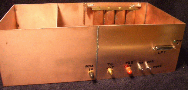
A good method for integrating the SLIMS is to use a mounting frame, using a 6 inch by 8 inch piece of .062 inch printed circuit board material (blue) with a top layer of copper. A hole is cut in this board for each SLIM. The hole size is the same size as the original SLIM pwb (ex. 1.2 x 1.2 in). Each SLIM has a fence around it's perimeter (except the Control Board), making it a little wider than the hole. The SLIM is then placed on the board frame, over the hole, and tack soldered in 4 places. This will make it very easy to remove the SLIM in the future. It makes the inside of a SLIM accessable from the top. The wire and coaxial connections are accessable from the bottom.
The coaxial cables are constructed and attached to the modules, on the bottom side. The wiring harness can be connectorized or the wires can be soldered point to point, without connectors. When completed, the perimeter of the carrier board will have room for drilling holes for mounting to the enclosure. The LPT connector on the Control Board will protrude through the enclosure's front panel. The power connector will be behind the enclosure's front panel, so a hole must be drilled in the enclosure to allow a power connector to mate with the Control Board's power connector. A .25 inch hole is drilled to allow the LED to protrude through the enclosure's front panel. .25 inch holes are drilled in the enclosure's front panel for mounting the Video Switches. The holes for MSA Input and Track Gen Output depend on the type of RF connector the builder prefers.
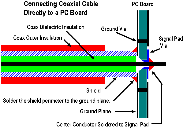
RF inputs and outputs of each module can be either SMA (or any small connector) or directly soldered, coaxial cable. I have been quite successful with direct connections using RG-085 and RG-141 hard pipe, and RG-188 soft coax. Click here to view a pictoral method of Coaxial Direct Connection to a PCB. I have gone so far as to remove the outer insulation of soft coax and "sweat" the outer braid with solder. This makes a 100% outer jacket. RF shielding is almost as good as hard pipe!
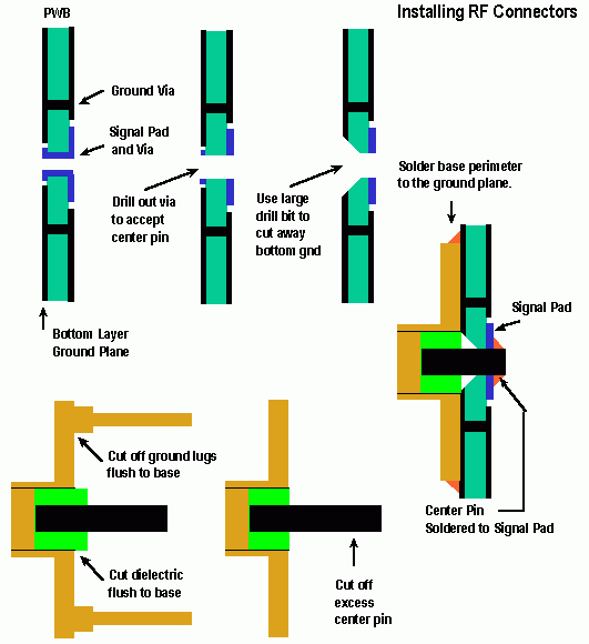
All of the SLIMs will accomodate the installation of RF connectors on the bottoms of their boards. However, none of them have ground vias for mounting ground posts. See a pictoral on how to modify an RF connector for installation on a SLIM. These items are also on the Construction Page.
Special Instructions while integrating the MSA:
When integrating any project, and especially the MSA, it is important to keep a documentation history. Create a 3 ring notebook called "MSA". Create several sections separated by Tabs. The first section "Integration", the others, one for each SLIM. Print out the current Block Diagram, Layout Diagram, Wiring Diagram, and the Schematics and parts list for each SLIM. Then, use a red pencil to update or change the documentation if necessary. You will have a complete, Baseline History of your system, in case there are any future design changes. I will expect this Web page and its contents to change as the MSA project continues. Also, if you ever have a question, as to performance, or are troubleshooting a problem, you can scan your document and send it to me for help. When I am asked a question, my first response is always, "What is your MSA configuration?". A picture is worth a gazillion words.
The following paragraphs will discuss any special considerations or modifications a SLIM must have when integrated into an MSA configuration. For full descriptions and construction of each SLIM, click on the SLIM part number in the paragraph's header. It will link to the Web page containing the full documentation for that SLIM, including pictures. Use your Browser's "BACK" button to return to this page.
Control Board using SLIM-CB-NV
The SLIM-CB-NV is designed with a Noise Filter Section. The noise filter is not required for any MSA configuration. All the components in that section can be omitted.
In the Voltage Converter section, only the +20 volts is used in the MSA. The -10v is not required in the MSA. Therefore, C18 and C19 can be omitted, although leaving them will not increase power consumption nor add extra noise.
Also note that the Voltage Regulator, U5, is mounted from the bottom side of the Control Board and should be bolted to the side of the main enclosure for heat sinking. If the Control Board is not next to the enclosure side panel, I suggest attaching a heat sink to U5. U5 power dissipation is about 3 watts, maximum.
Control Boards previous to Rev C can be updated by adding the appropriate resistors and capacitors. Click on the above link for the modifications.
When installing the signal wiring harness, the common signal (DATACLK) is used to command up to 5 different modules. These wires MUST be installed as a "star" configuration. That is, all the wires are tied to a single common point on the Control Board, P1- pin 2 and then tied to the appropriate modules individually. It would be best to have all the wires of equal length. If the modules are "daisy-chained", the signal reflection can cause multiple commanding.
When the 25 pin LPT connector is attached to the pwb, only the pins are soldered. The shell is not soldered, so solder a wire or strap from the shell to the perimeter ground of the pwb. This decreases computer noise from entering the MSA.
Several builders have complained of spurious responses that are 8 to 10 KHz above and below the signal of interest (and their harmonics). This has been attributed to poor quality capacitors (ESR, effective serial resistance) used in the 20 volt multiplier. Specifically, C21, C24, and C25. The cure is to "double up" the capacitors. That is, add (piggyback) another 10 ufd capacitor across one or more of these capacitors.
Mixer 1 using SLIM-MXR-1
Special Caution: Since the MSA input is directly coupled to Mixer 1, the I port diodes of the mixer can be destroyed by applying a signal with a DC voltage. It can also be destroyed by a too-high RF input signal. Good rule of thumb to prevent mixer damage: maximum input signal should not be greater than the specified L Port power (+7 dBm). To prevent accidental input over-voltage, a 3 dB to 10 dB attenuator can be installed in the I Port circuit. This is shown as a resistor in the MSA Block Diagram and as R15 in the SKSLIM-MXR-1 schematic. A pi-type attenuator can be added using the pads, X14, X15, and X17. This will also improve input impedance matching. It will, however, shift the Dynamic Range of the MSA to accept higher input signals.
Once the MSA has been fully tested and its functionality verified, the user may find that the Spectrum Analyzer's Magnitude Gain versus Frequency may have an abrupt change at some frequency below 400 MHz. This is due to the Coaxial Cavity Filter path creating a mismatch to Mixer 1 at frequencies other than the prescribed First Intermediate Frequency of 1013.3 MHz. The actual frequency is dependent on the length of the coaxial path from Mixer 1 (J3) to the Coaxial Cavity Filter. The abrupt change in gain will not affect the accuracy of the MSA. This mismatch can be minimized with a simple modification to the SLIM-MXR-1 module. This modification is optional to the user, and not essential for accurate operation. The modification is adding a series 1 pfd capacitor and 50 ohm resistor from the ADE-11X's R port to ground. See the SLIM-MXR-1 page for modification information.
Mixer 2 using SLIM-MXR-2
No special considerations are required.
Mixer 3 using SLIM-MXR-3
MXR-3 is used only when the Tracking Generator is added to the Basic MSA.
Its modification from Rev 0 to Rev A needs mentioning here. The Mixer 3, J3 is operating at a fixed frequency of 1024 MHz. The ADE-11X R port impedance is not exactly, 50 ohms at 1024 MHz. Matching the mixer's R port, to the internal 14 dB attenuator, can be greatly improved by adding a 2.0 or 2.2 pF chip capacitor in the C9 position. This is on the ADE-11X, pin 3 to ground.
Mixer 4 using SLIM-MXR-4
MXR-4 is used only when the MSA/TG is extended into a VNA. No special considerations are required.
1013.3 MHz Coaxial Cavity Filter : Cavity Filter Construction Page
When constructing this filter, leave enough semi-rigid cable attached to the filter to connect to Mixer 1 and Mixer 2 of the MSA. I might even suggest that the builder construct this filter last, to insure a proper "fit" into the MSA. I mounted the Coaxial Cavity Filter vertically, and in the rear of the enclosure. It could be mounted anywhere in the enclosure and the coaxial lines can be any length. The filter is bi-directional and its orientation is not important. It does not need to be critically tuned before integration into the MSA. Critical tuning will be accomplished during the Initial Set-Up procedure.
DDS 1, using SLIM-DDS-107
The MSA configuration requires only one output from DDS 1, the square wave output from the Squaring Buffer, J4. It is used as the reference clock input to J1 of PLO 1. However, I would suggest that J3 (DDS B) be populated with a pwb RF connector, or a coaxial cable running to a connector on the front panel of the MSA assembly. It can be used as a frequency source for other purposes. The DDS B output will have an amplitude of approximately -8 dBm. The fundamental signal will also contain alias frequencies and many spurious frequencies. I will publish some experiments, using this output, at a later date.
Omit or remove R3, the 49.9 ohm load resistor. This will allow a full 5 volt pp Master Clock, and the reflection will be retrurned to the Master Clock Module and be absorbed by the 33 ohm series driving resistor.
Update 7-26-09 The SLIM-DDS-107 has been changed to Revision D. Previous versions of the DDS can be modified for this change. A low pass filter network has been added to the output of the DDS to suppress harmonic generation within the receiving module, PLO-1. Modification is not essential for MSA operation, but it does improve its spur characteristics.
DDS 3, using SLIM-DDS-107
The DDS 3 is required only when adding the Tracking Generator or VNA to the Basic MSA. It is built and configured identically to the DDS 1. Like DDS 1, the spare output J3 of DDS 3 can be brought out to the front panel for other experimentation.
Update 7-26-09 The SLIM-DDS-107 has been changed to Revision D. Previous versions of the DDS can be modified for this change. A low pass filter network has been aded to the output of the DDS to suppress harmonic generation within the receiving module, the PLO-1. Modification is not essential for MSA operation, but it does improve its spur characteristics.
PLO 1 using SLIM-PLO-1
A fully configured SLIM-PLO-1 has two active outputs, J2 and J3. Both are used for the MSA/TG, Build Level 2. The Basic MSA requires only one output from the PLO 1. However, I suggest you completely populate the module to take advantage of multiple Functions of the Basic MSA. The unused output can be brought out to the Front or Rear Panel and used for other experiments. Its output is 1000 MHz to 2000 MHz. at +10 dBm. Load it with 50 ohms if not used.
The SLIM-PLO-1 has been changed to Revision C to modify the PLL's Loop Filter. Previous versions of the PLO can be modified for this change. Modification is not essential for MSA operation, but it does improve its spur characteristics.
Updated 7-26-09 When constructing SLIM-PLO-1 for the SLIM MSA system, install C27 and R12. This changes my original suggestion of deleting them. This 50 ohm loading will suppress harmonic products that are created within the PLL.
Updated 7-26-09 Advisory: When connecting the +20 volts from P1-6 to the Control Board P23-2, connect a ground wire from P1-1 to Control Board P23-1. This will minimize power supply noise.
PLO 3 using SLIM-PLO-1
PLO-3 is used when the Tracking Generator is added to the Basic MSA. When integrating only the Tracking Generator, only one buffer amplifier is required to drive Mixer 3. However, I would suggest fully constructing PLO-3 with both buffer amplifiers. The spare buffer amplifier output can be brought out to the front or rear panel and used for other experiments. Its output is 1000 MHz to 2000 MHz. at +10 dBm. Load it with 50 ohms if not used. If the MSA/TG is extended into the VNA configuration, both buffer amplifiers are used.
The SLIM-PLO-1 has been changed to Revision C to modify the Loop Filter in the Phase Locked Loop. Previous versions of the PLO can be modified for this change. Modification is not essential for MSA operation, but it does improve its spur characteristics.
Update 7-26-09 When constructing SLIM-PLO-1 for the SLIM MSA system, install C27 and R12. This changes my original suggestion of deleting them. It will suppress harmonic products that are created within the PLL.
Normally, the J2 output of PLO 3 is driving the J1 input of Mixer 3. For 2G Band operation (1-2 GHz), the output of PLO 3 may be used as a high level Tracking Generator Output. If this option is used, bring the J2 output of PLO 3 to the Front Panel of the MSA and label it "PLO 3 Out, 1-2 GHz, +10 dBm". Also, bring the J1 input of Mixer 3 to the Front Panel so that the two connectors can be cross coupled for 1G and 3G Band operation.
Updated 7-26-09 Advisory: When connecting the +20 volts from P1-6 to the Control Board P24-2, connect a ground wire from P1-1 to Control Board P24-1. This will minimize power supply noise.
PLO 2 using SLIM-PLO-2
A fully configured SLIM-PLO-2 has two active outputs, J2 and J3. The Basic MSA requires only one output from the PLO 2, used as the LO drive for Mixer 2, at +10 dBm. However, I highly suggest you completely populate the PLO 2 module to take advantage of multiple Functions of the Basic MSA.
When constructing SLIM-PLO-2 for the SLIM MSA system, omit C27 and R12. The Master Oscillator's driver to this circuit will absorb the mismatch reflection. This may seem a like poor design but it is valid. It improves the noise performance of PLL 2.
Final I.F. Xtal Filter, or Resolution Bandpass Filter. Many Options.
The Final Xtal Filter determines the Resolution Bandwidth of the MSA. Steep slopes and out of band rejection is a must for good selectivity. There are many options for the MSA builder. Bandwidths can be chosen to be as narrow as 100 Hz or as wide as 2 MHz (it does not have to be a crystal filter). Since this is the choice of the builder, I will not specify any particular filter. Here are a few suggestions:
PWB-MCF. A printed wiring board that will accommodate a variety of Monolithic Crystal Filters (MCF) which can be chosen by the builder. Center frequency and resolution bandwidth is determined by the MCF. Here are some SLIM filters using this PWB, and are described on the PWB-MCF Web Page:
SLIM-MCF-FL096. Center frequency is 10.695 Mhz, bandwidth is 3.8 KHz. This is the design I used when building and testing the first SLIM MSA/TG/VNA verification unit. It is an 8 pole filter and has a loss of about 4 dB. The filter is from an old CB radio and is probably made by Uniden. However, I can not find it for sale anywhere.
SLIM-MCF-L024. Center frequency is 10.695 MHz, bandwidth is 2.2 KHz. The monolithic crystal filter is from U.S. Electronics, part no. 10L024A. I designed this module, "blind". That is, I don't have this filter to test. However, I have tested several similar filters, taken from some single sideband CB radios, with similar characteristics. This is the only filter I could find that is on the open market. All the filters I have experimented with are not offered to the public. The problem is, U.S. Electronics sells in lots of 1000. I (we) must find a viable alternative to this filter. That is why the term "place holder" is in the title.
QMF 10725. This Hi-Q, MCF is too large to fit on the PWB-MCF board, but I placed its test data there, for information only. It is an 8 pole MCF with a bandwidth of 7.5 KHz. The QMF 10713 has 15 KHz bandwidth, with the same impedance specification. Two MSA builders have reported excellent results with this filter, acquired on E-Bay.
PWB-CLF-5. A printed wiring board that will accommodate up to 5 crystals, for constructing a Crystal Ladder Filter. Center frequency and resolution bandwidth is determined by the builder. This design is excellent for very narrow bandwidth filters, less than 1 KHz. This Web page has a few examples.
I will soon add a final filter using cascaded filters that are available from Digikey and Mouser.
Optional Filter Bank Selector using SLIM-2P4T
The Final I.F. Filters in the previous paragraph can be used individually by manually connecting each filter as required. An optional Filter Bank Selector can be used to select one of four filter paths using the MSA software control. This option is not specifically shown in the MSA Block Diagram, but includes the four Final Filter Paths (the filters) and the SLIM-2P4T Switch.
Log Detector using SLIM-LD-8306
The SLIM-LD-8306 has two outputs. The Mag(nitude) Volts Output at J2 is used in the Basic MSA. The second output, Lim(ited) IF Out on J3, is not used in the Basic MSA. It is used when the MSA is expanded to the MSA/VNA configuration. If you plan not to use this output, do not install R4-R6, and C12. This will disable the limiter section of the I.C. However, I suggest you completely populate the module to take advantage of multiple Functions of the Basic MSA.
After much testing of the Log Detector, I have concluded that its noise floor is somewhat dependent on its operating temperature. If your MSA will use a very narrow Final Xtal Filter (less than 2 KHz), I suggest locating this module in the coolest spot in your assembly. Under a fan or next to a wall, away from excess heat. You will not see any difference when using wider bandwidths.
For the adventurous builder, there is an optional modification to the Log Detector to improve its dynamic range. It is described on the bottom of SLIM-LD-8306 .
A to D Converter, using either a 12 or 16 Bit Serial A to D Converter:
16 Bit Serial A to D Converter using SLIM-ADC-16
The SLIM-ADC-16 design has two A/D circuits, but only one is used for the Basic MSA. The other is used when the MSA is expanded to VNA operation. For the Basic MSA, the "PHA VOLTS" section can be left unpopulated. That would be U3 and all of it's supporting components. However, I suggest you completely populate the module to take advantage of multiple Functions of the Basic MSA. When used for the Basic MSA or MSA with Tracking Generator only, no other special considerations are required for the A to D Converter. Power to the A to D Converter can be supplied by the +10v distribution on the Control Board (P9). However, for best Phase detection accuracy, the following Optional Power Configuration is recommended.
Optional Power Configuration for VNA operation. (Updated 12-20-14) When the VNA extension is integrated, the +10 volt power from the Control Board is not used for the A to D Converter. Instead, +5v power is supplied to the to the A to D Converter from the Phase Detector Module. This is a regulated +5 volts created within the Phase Detector Module and output on its P2 connector. This option improves the Phase Measurement accuracy of the VNA. For this option, both the SLIM-ADC-16 and SLIM-PDM must be modified:
Modification procedure to SLIM-ADC-16: Remove (or do not install) U1, the 5 volt regulator. Add a jumper wire between the remaining pads associated with U1 pin 3 and U1 pin 1. When interconnecting the modules in the VNA system, connect SLIM-ADC-16, P1 pins 1 and 2 to SLIM-PDM, P2, pins 1 and 2. This allows both modules to use the same 5 volt source as a common reference. If this modification is performed after an MSA Magnitude calibration, the calibration must be retaken, due to a probable change in reference voltage.
12 Bit Serial A to D Converter using SLIM-ADC-12
The SLIM-ADC-12 is an option to the 16 Bit SLIM. It is less expensive to build, yet still has good resolution. This module has two A/D circuits, but only the "Mag Volts" section is used in the Basic MSA. The other section is used when the MSA is expanded to VNA operation. For a Basic MSA, the "PHA VOLTS" section can be unpopulated. That would be U3 and all of it's supporting components. However, I highly suggest you completely populate the module to take advantage of multiple Functions of the Basic MSA.
Modification to SLIM-ADC-12 for VNA extensiton. The "PHA VOLTS" (J2) is designed for an input dynamic range of +1 volt to +4 volts. For use in the SLIM MSA/VNA, the range must be changed to 0 volts to +5 volts, the expected output of the Phase Detector Module. The reason for this change is that the designed voltage divider in the SLIM-ADC-12 can create as much as a 2% error in phase accuracy. This equates to an error of 7.2 degrees. Therefore, a modification to the SLIM-ADC-12 is required:
Modification procedure to SLIM-ADC-12: If the SLIM-ADC-12 has been fully assembled, just remove R6, a 665 ohm resistor. If you have not assembled the SLIM-ADC-12, delete R6, change R7 to 0 (zero) ohms, and delete C17 and C18. With this mod, the resolution of the SLIM-ADC-12 is 360/4095 = .0879 degrees per bit.
Optional Power Configuration for VNA operation. When the VNA extension is integrated, there is an optional configuration to consider. This option changes the way power is supplied to the to the A to D Converter. Instead of the Control Board supplying +10 volts to the A to D Converter, the Phase Detector Module will supply a regulated +5 volts to the A to D Converter. This option will improve the Phase Measurement accuracy of the VNA. For this option, the SLIM-ADC-12 and SLIM-PDM must be modified:
Modification procedure to SLIM-ADC-12: Remove (or do not install) U1, the 5 volt regulator. Add a jumper wire between the remaining pads associated with U1 pin 3 and U1 pin 1. When interconnecting the modules in the VNA system, connect SLIM-ADC-12, P1 pins 1 and 2 to SLIM-PDM, P2, pins 1 and 2. This allows both modules to use the same 5 volt source as a common reference. If this modification is performed after an MSA Magnitude calibration, the calibration must be retaken, due to a probable change in reference voltage.
16 Bit Serial A to D Converter with Multiplexer using SLIM-ADCMUX
The SLIM-ADCMUX design has a 16 bit ADC with an 8 channel analog multiplexer. It is an optional replacement for the SLIM-ADC-16.
Channel commanding (CH 0 to CH 7) is accomplished by using three command signals from the Control Board:
CB-P3-2 to ADCMUX-P11-2, CB-P3-3 to ADCMUX-P10-2, and CB-P3-3 to ADCMUX-P9-2.
Analog Inputs:
Analog input CH 0 is Magnitude: Log Detector J2 to ADCMUX P13-2 (P13-1 is ground). Suggest using twisted wire pair.
Analog input CH 1 is Phase: Phase Detector J3 to ADCMUX P14-2 (P14-1 is ground). Suggest using twisted wire pair.
Channels 2 thru 7 are reserved for upgrades to the MSA.
When used as a multiplexer with ADC (to replace the SLIM-ADC-16) any video filtering is placed directly on the Multiplexer inputs as desired. For Mag and Phase, either the Video Filter Module or the mechanical switches (with capacitors) is placed on the Multiplexer inputs, CH 0 and CH 1.
ADC Interfacing, 2 inputs, 1 output:
Convert signal, input (ADCONV): CB-P3-9 to ADCMUX-P7-2
Serial Clk signal, input (ADSERCLK): CB-P3-8 to ADCMUX-P8-2
Serial Data, output (WAIT): ADCMUX-P6-2 to CB-P25-4 (MAGNITUDE or PHASE DATA)
If the MSA does not have VNA capability, power to the A to D Converter (ADCMUX-P16) is supplied by the +10v distribution from the Control Board (P9) to ADCMUX-P16. But for VNA, and best Phase detection accuracy, the following Optional Power Configuration is recommended.
Optional Power Configuration for VNA operation. When the VNA extension is integrated, the +10 volt power from the Control Board is not used for the A to D Converter. Instead, +5v power is supplied to the to the A to D Converter from the Phase Detector Module. This is a regulated +5 volts created within the Phase Detector Module and output on its P2 connector. This option improves the Phase Measurement accuracy of the VNA. For this option, the SLIM-ADCMUX must be modified:
Modification procedure to SLIM-ADCMUX: Remove (or do not install) U1, the 5 volt regulator. When interconnecting the modules in the VNA system, connect SLIM-ADCMUX, P17 pins 1 and 2 to SLIM-PDM, P2, pins 1 and 2. This allows both modules to use the same 5 volt source as a common reference. If this modification is performed after an MSA Magnitude calibration, the calibration must be retaken, due to a probable change in reference voltage.
Master Oscillator using SLIM-MO-64
The SLIM-MO-64 has three outputs, all used for Tracking Generator addition. Only two are used in the Basic MSA. If an output is not used, leave it unterminated. Or, to conserve power in the Basic MSA, U6, R3, R6, and C9 could be deleted. However, I highly suggest you completely populate the module to take advantage of multiple Functions of the Basic MSA.
I.F. Amplifier using SLIM-IFA-33
No special considerations or modifications are required for MSA integration.
Optional RF/Buffer Amplifier using SLIM-RFA-1
This SLIM is optional and only used with the Tracking Generator or VNA builds. Only one section of the Amplifier is used. Its use will increase the reverse isolation of Mixer 3 back to PLO 2. For best VNA results below 2 MHz, this optional buffer is desirable.
The PWB can be sliced in half and both sections built, resulting in two independent buffers. The second can be placed between PLO 1-J2 and Mixer 4-J1. It will increase the reverse isolation and improve spurious responses associated with the 10.7 MHz I.F. Do not use both in the same module, as cross-coupling will be high.
PDM, Phase Detector Module, using SLIM-PDM
The SLIM-PDM is used only when expanding the MSA/TG into the VNA. If the PDM is used to source its regulated +5 volts to the SLIM-ADC (AtoD Converter Module), install both FBx and FB2. No other special considerations or modifications are required for MSA/VNA integration.
Updated 11-20-10: The SLIM-PDM-revB has been modified into rev C, to improve the stability of the one-shots (U8 and U9). Two additional capacitors, C24 and C25 (22 pfd) are added to the schematic and added to the SLIM assembly. A new PWB is not released. PWB-PDM Rev A is still current. The layout is modified to LAYSLIM-PDM-revC. The schematic is modified from SKSLIM-PDM Rev B to SKSLIM-PDM Rev C.
Updated 1-24-16: A new PWB is now released as PWB-PDM Rev C. Pads for the two additional capacitors, C24 and C25 (22 pfd) are added.
Specifications for the Basic MSA (Basic Spectrum Analyzer)
Dual Conversion Topology 1013.3 MHz first I.F., 10.7 MHz final I.F.
Frequency of Operation 10 KHz to 1 GHz, 1-2 GHz (2G Path Option), and 2-3 GHz
Frequency Resolution < 3 Hz
Sensitivity <-110 dBm, dependent on Resolution BW
Dynamic Range greater than 85 dB, dependent on Resolution BW
Amplitude Resolution 0.04 dB or better
Resolution Bandwidths suggested: 300 Hz, 3 KHz, 30 KHz, 300 KHz Final Filters
Noise Figure <23 dB
Phase Noise <-91 dBc/Hz, 10 KHz from carrier
Image Rejection In-Band Image Rejection better than -100 dBc
IM Distortion Two tone, -60 dBc or better
Max Input Signal RF = +13 dBm; DC= 20 ma. (These are maximums to prevent damage to Mixer 1)
Number of SLIMs 11 modules, plus coaxial cavity filter
Specifications for the Tracking Generator Addition, MSA/TG :
Output Frequency, Level < 1 Hz to 1000 MHz @ -11 dBm, +/- 1 dB (difference)
2000 MHz to 3000 MHz @ -14 dBm, +/- 2 dB (sum)
1000 MHz to 2000 MHz @ -20 dBm, +/- 2 dB (feedthru)
1000 MHz to 2000 MHz @ +9 dBm, +/- 1 dB (bypass option)
Number of SLIMs 3 additional to Basic MSA
Specifications for the Vector Network Analyzer Extension, MSA/TG/VNA :
Frequency of Operation same as SA (0-1 GHz, 1-2 GHz, 2-3 GHz)
Instantaneous Dynamic Range greater than 70 dB
Phase Resolution 0.1 degrees or better
Number of SLIMs 2 additional to MSA/TG
Cost of the MSA using SLIMs
We have found several vendors selling SMA connectors on E-Bay for $0.50 each. Therefore I have modified the cost analysis. Approximate cost ($USA) of the MSA, fully built boards with connectors, or without connectors:
| SLIMs | Full Boards | w/o Conns |
| SLIM-ADC-12 | 24.96 | 23.96 |
| SLIM-CB-NV | 29.82 | 29.82 |
| SLIM-DDS-107 | 34.87 | 33.37 |
| SLIM-IFA-33 | 13.56 | 11.56 |
| SLIM-LD-8306 | 32.44 | 30.94 |
| SLIM-MCF-L024 | 17.36 | 16.36 |
| SLIM-MO-64 | 12.43 | 10.93 |
| SLIM-MXR-1 | 7.91 | 6.41 |
| SLIM-MXR-2 | 9.03 | 7.53 |
| SLIM-PLO-1 | 55.82 | 54.32 |
| SLIM-PLO-2 | 36.80 | 35.3 |
| Total for SLIMs Only | $275.00 | $260.50 |
Added costs of other materials:
| Other
Materials |
w/Conns |
wo Conns |
| 28 in. RG-085 @ $5 ft. |
11.67 | 11.67 |
| 23 coax conns @ $.50 |
11.50 | 0 |
| Cavity Filter |
5.00 | 4 |
| Wall Wart Pwr Supply |
15 | 15 |
| Front Panel Conns. |
6 | 6 |
| Enclosure Box |
20 | 20 |
| Total for
Basic MSA |
$344.17 | $317.17 |
Added cost for Tracking Generator Addition:
| SLIMs | Full Boards | wo Conns |
| SLIM-MXR-3 | 9.03 | 7.53 |
| SLIM-PLO-3 | 55.82 | 54.32 |
| SLIM-DDS-107 | 34.87 | 33.37 |
| Total for
MSA/TG |
$443.89 | $412.39 |
Added cost for VNA Extension:
| SLIMs | Full Boards | wo Conns |
| SLIM-MXR-4 | 9.03 | 7.53 |
| SLIM-PDM | 10.94 |
9.44 |
| Total for
MSA/TG/VNA |
$463.86 | $429.36 |